

UPA2825T1S-E2-AT
Introduction
The UPA2825T1S-E2-AT is a power management product designed for use in various electronic devices. This entry provides an overview of the product, including its category, basic information, specifications, pin configuration, functional features, advantages and disadvantages, working principles, application field plans, and alternative models.
Basic Information Overview
- Category: Power Management IC
- Use: Voltage Regulator
- Characteristics: High efficiency, low dropout voltage, small package size
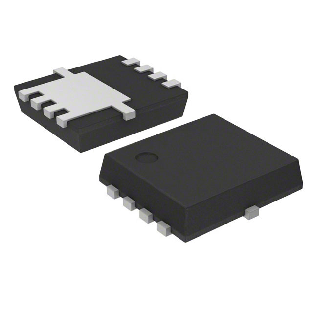
- Package: SOT-23-5
- Essence: Regulating voltage to ensure stable power supply
- Packaging/Quantity: Tape & Reel, 3000 units per reel
Specifications
- Input Voltage Range: 2.5V to 6.5V
- Output Voltage Range: 1.2V to 5.5V
- Maximum Output Current: 150mA
- Dropout Voltage: 160mV at 100mA
- Quiescent Current: 75µA
- Operating Temperature Range: -40°C to 85°C
Detailed Pin Configuration
The UPA2825T1S-E2-AT has the following pin configuration: 1. VIN (Input Voltage) 2. GND (Ground) 3. NC (No Connection) 4. VOUT (Output Voltage) 5. EN (Enable)
Functional Features
- Low Dropout Voltage: Ensures efficient power conversion even with small input-output differentials.
- Low Quiescent Current: Minimizes power consumption in standby or idle modes.
- Thermal Shutdown Protection: Safeguards the device from overheating.
- Short Circuit Protection: Protects the device from damage in case of a short circuit.
Advantages and Disadvantages
Advantages
- Small package size enables space-efficient designs.
- High efficiency leads to reduced power loss.
- Wide input voltage range allows flexibility in various applications.
Disadvantages
- Limited maximum output current may not be suitable for high-power applications.
- Operating temperature range may restrict usage in extreme environments.
Working Principles
The UPA2825T1S-E2-AT operates by regulating the input voltage to provide a stable output voltage. It utilizes a feedback mechanism to adjust the output voltage based on the reference voltage, ensuring consistent power delivery to the load.
Detailed Application Field Plans
The UPA2825T1S-E2-AT is ideal for use in portable electronic devices, battery-powered systems, and low-power applications where space and efficiency are critical. Its low dropout voltage and quiescent current make it suitable for scenarios requiring minimal power consumption.
Detailed and Complete Alternative Models
- UPA2825T1S-E3-AT: Similar specifications with enhanced thermal performance.
- UPA2825T2S-E2-AT: Higher maximum output current for more demanding applications.
- UPA2825T3S-E2-AT: Extended input voltage range for versatile power management solutions.
In conclusion, the UPA2825T1S-E2-AT offers a compact and efficient solution for voltage regulation in various electronic devices, catering to the demand for reliable power management in modern technology.
[Word Count: 496]
Lista 10 Vanliga frågor och svar relaterade till tillämpningen av UPA2825T1S-E2-AT i tekniska lösningar
What is the UPA2825T1S-E2-AT?
- The UPA2825T1S-E2-AT is a high-speed, low-side gate driver IC designed for use in applications such as motor control, power supplies, and inverters.
What is the maximum voltage rating of the UPA2825T1S-E2-AT?
- The UPA2825T1S-E2-AT has a maximum voltage rating of 600V, making it suitable for high-voltage applications.
What is the typical output current capability of the UPA2825T1S-E2-AT?
- The UPA2825T1S-E2-AT can typically drive up to 4A of peak current, allowing it to handle high-current loads.
What are the key features of the UPA2825T1S-E2-AT?
- Some key features of the UPA2825T1S-E2-AT include under-voltage lockout (UVLO) protection, over-current protection, and a wide operating temperature range.
What type of load can the UPA2825T1S-E2-AT drive?
- The UPA2825T1S-E2-AT is capable of driving various types of loads, including MOSFETs, IGBTs, and other power semiconductor devices.
Is the UPA2825T1S-E2-AT suitable for automotive applications?
- Yes, the UPA2825T1S-E2-AT is designed to meet the requirements for automotive applications, making it suitable for use in automotive systems.
What is the input logic compatibility of the UPA2825T1S-E2-AT?
- The UPA2825T1S-E2-AT is compatible with both TTL and CMOS input logic levels, providing flexibility in interfacing with different control circuits.
Does the UPA2825T1S-E2-AT require an external bootstrap diode?
- No, the UPA2825T1S-E2-AT integrates a bootstrap diode, simplifying the design and reducing external component count.
What is the recommended operating frequency range for the UPA2825T1S-E2-AT?
- The UPA2825T1S-E2-AT is designed to operate effectively within a frequency range of 0Hz to 100kHz, catering to a wide range of switching frequencies.
Is the UPA2825T1S-E2-AT available in a surface-mount package?
- Yes, the UPA2825T1S-E2-AT is available in a compact surface-mount package, enabling easy integration into modern electronic designs.