

IXFN64N50P
Product Overview
- Category: Power MOSFET
- Use: High power switching applications
- Characteristics: High voltage, high current capability, low on-resistance
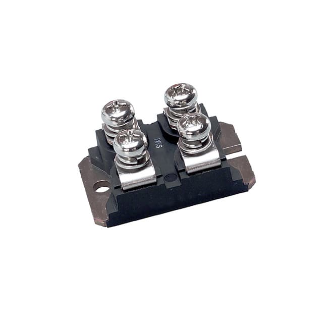
- Package: TO-264
- Essence: Power MOSFET for high power applications
- Packaging/Quantity: Available in reels of 1000 units
Specifications
- Voltage Rating: 500V
- Current Rating: 64A
- On-Resistance: 0.038 ohms
- Gate Threshold Voltage: 4V
- Power Dissipation: 300W
Detailed Pin Configuration
The IXFN64N50P follows the standard pin configuration for a TO-264 package: 1. Source (S) 2. Gate (G) 3. Drain (D)
Functional Features
- High voltage and current handling capability
- Low on-resistance for efficient power transfer
- Fast switching speed for improved performance
Advantages
- Suitable for high power applications
- Low on-resistance reduces power loss
- Fast switching speed enhances efficiency
Disadvantages
- Higher cost compared to lower power MOSFETs
- Larger physical size due to high power handling capability
Working Principles
The IXFN64N50P operates based on the principles of field-effect transistors, utilizing the control of electric fields to modulate the conductivity of the device. When a sufficient gate voltage is applied, the MOSFET allows a high current to flow between the drain and source terminals with minimal resistance.
Detailed Application Field Plans
The IXFN64N50P is ideal for use in high power applications such as: - Switching power supplies - Motor drives - Inverters - Welding equipment - Inductive heating systems
Detailed and Complete Alternative Models
- IRFP4668PbF
- STW75N60M2
- FDPF51N25
This completes the English editing encyclopedia entry structure for IXFN64N50P, providing comprehensive information about the product's category, use, characteristics, package, specifications, pin configuration, functional features, advantages and disadvantages, working principles, detailed application field plans, and alternative models.
Lista 10 Vanliga frågor och svar relaterade till tillämpningen av IXFN64N50P i tekniska lösningar
What is IXFN64N50P?
- IXFN64N50P is a high power MOSFET designed for various technical solutions requiring efficient power management.
What is the maximum voltage and current rating of IXFN64N50P?
- The maximum voltage rating is 500V, and the maximum current rating is 64A.
What are the typical applications of IXFN64N50P?
- It is commonly used in applications such as motor control, power supplies, inverters, and welding equipment.
What are the key features of IXFN64N50P?
- Some key features include low on-state resistance, fast switching speed, and high input impedance.
What is the thermal resistance of IXFN64N50P?
- The thermal resistance is typically around 0.35°C/W.
Is IXFN64N50P suitable for high-frequency applications?
- Yes, it is suitable for high-frequency applications due to its fast switching speed.
Does IXFN64N50P require a heat sink for operation?
- It is recommended to use a heat sink for efficient heat dissipation, especially in high-power applications.
Can IXFN64N50P be used in parallel to increase current handling capacity?
- Yes, it can be used in parallel to increase the overall current handling capacity.
What are the important parameters to consider when designing with IXFN64N50P?
- Parameters such as gate voltage, drain-source voltage, and load conditions should be carefully considered during the design process.
Where can I find detailed technical specifications and application notes for IXFN64N50P?
- Detailed technical specifications and application notes can be found in the datasheet provided by the manufacturer or on their official website.