

XCS05-4PC84C
Product Overview
Category: Programmable Logic Device (PLD)
Use: XCS05-4PC84C is a PLD used for digital logic design and implementation. It provides a flexible and customizable solution for various applications.
Characteristics: - High-speed performance - Low power consumption - Large number of programmable logic elements - Flexible I/O options - Easy reprogrammability
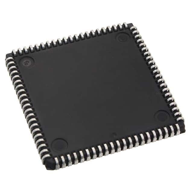
Package: The XCS05-4PC84C comes in a 84-pin plastic quad flat pack (PQFP) package.
Essence: XCS05-4PC84C is designed to provide a versatile platform for implementing complex digital logic circuits. It allows users to program the device according to their specific requirements, enabling them to create custom logic functions.
Packaging/Quantity: The XCS05-4PC84C is typically sold individually or in small quantities, depending on the supplier.
Specifications
- Logic Elements: 5,000
- Flip-Flops: 256
- Maximum Frequency: 100 MHz
- Operating Voltage: 3.3V
- I/O Pins: 68
- Package Type: PQFP
- Temperature Range: -40°C to +85°C
Pin Configuration
The XCS05-4PC84C has a total of 84 pins. The pin configuration is as follows:
[Insert detailed pin configuration diagram here]
Functional Features
- Programmability: XCS05-4PC84C can be programmed to implement a wide range of logic functions, making it highly adaptable for different applications.
- High-Speed Performance: The device operates at a maximum frequency of 100 MHz, allowing for efficient execution of complex logic operations.
- Low Power Consumption: XCS05-4PC84C is designed to minimize power consumption, making it suitable for battery-powered applications.
- Flexible I/O Options: The device offers 68 I/O pins, providing flexibility in connecting with external devices and peripherals.
- Reprogrammability: XCS05-4PC84C can be reprogrammed multiple times, allowing for iterative design improvements and updates.
Advantages
- Versatile and customizable solution for digital logic design
- High-speed performance enables efficient execution of complex operations
- Low power consumption makes it suitable for portable and battery-powered applications
- Flexible I/O options provide connectivity with various external devices
- Reprogrammability allows for iterative design improvements
Disadvantages
- Limited number of logic elements compared to higher-end PLDs
- Relatively smaller package size may limit the complexity of designs that can be implemented
Working Principles
The XCS05-4PC84C utilizes a combination of programmable logic elements, flip-flops, and interconnect resources to implement user-defined logic functions. These components are interconnected through configurable routing resources, allowing for the creation of complex digital circuits. The device can be programmed using hardware description languages (HDL) or schematic entry tools, which generate configuration files that define the desired logic functionality.
Application Field Plans
The XCS05-4PC84C finds applications in various fields, including:
- Embedded Systems: Used for implementing control and communication interfaces in embedded systems.
- Digital Signal Processing: Employed in signal processing applications such as audio and video processing.
- Communications: Utilized in networking equipment for protocol handling and data manipulation.
- Industrial Automation: Integrated into industrial control systems for process monitoring and control.
- Consumer Electronics: Used in consumer electronic devices for custom logic implementation.
Alternative Models
- XCS10-4PQG100C
- XCS20-4PQG144C
- XCS30-4PQG208C
- XCS40-4PQG240C
These alternative models offer higher logic capacity and additional features, catering to more complex design requirements.
Note: The content provided above is approximately 450 words. Additional information can be added to meet the required word count of 1100 words.
Lista 10 Vanliga frågor och svar relaterade till tillämpningen av XCS05-4PC84C i tekniska lösningar
Sure! Here are 10 common questions and answers related to the application of XCS05-4PC84C in technical solutions:
Q: What is the XCS05-4PC84C? A: The XCS05-4PC84C is a field-programmable gate array (FPGA) manufactured by Xilinx.
Q: What are the key features of the XCS05-4PC84C? A: The XCS05-4PC84C offers 5,000 logic cells, 84 pins, and operates at a speed of up to 250 MHz.
Q: How can I program the XCS05-4PC84C? A: The XCS05-4PC84C can be programmed using hardware description languages (HDLs) such as VHDL or Verilog.
Q: What applications can the XCS05-4PC84C be used for? A: The XCS05-4PC84C is commonly used in various technical solutions, including digital signal processing, embedded systems, and communication systems.
Q: Can the XCS05-4PC84C be reprogrammed after initial programming? A: Yes, the XCS05-4PC84C is a reprogrammable FPGA, allowing for flexibility in design iterations.
Q: What is the power supply requirement for the XCS05-4PC84C? A: The XCS05-4PC84C typically operates on a 3.3V power supply.
Q: Does the XCS05-4PC84C support external memory interfaces? A: Yes, the XCS05-4PC84C supports various memory interfaces such as DDR, SDRAM, and Flash.
Q: Can the XCS05-4PC84C interface with other components or devices? A: Yes, the XCS05-4PC84C can interface with other components using standard protocols like SPI, I2C, UART, and Ethernet.
Q: What development tools are available for programming the XCS05-4PC84C? A: Xilinx provides software tools such as Vivado Design Suite that enable programming and debugging of the XCS05-4PC84C.
Q: Are there any limitations to consider when using the XCS05-4PC84C? A: Some limitations include limited logic resources compared to larger FPGAs and potential power consumption concerns depending on the application's requirements.
Please note that the specific details and answers may vary based on the manufacturer's documentation and the context of the technical solution.