

XC95288XV-7CS280C
Product Overview
Category
XC95288XV-7CS280C belongs to the category of programmable logic devices (PLDs).
Use
This product is commonly used in digital circuit design and implementation. It provides a flexible and customizable solution for various applications.
Characteristics
- Programmable: The XC95288XV-7CS280C can be programmed to perform specific functions, allowing for versatility in circuit design.
- High-density: This PLD offers a high number of logic cells, enabling complex designs to be implemented.
- Low power consumption: The device is designed to operate efficiently with minimal power requirements.
- Fast operation: With its advanced architecture, the XC95288XV-7CS280C delivers high-speed performance.
Package
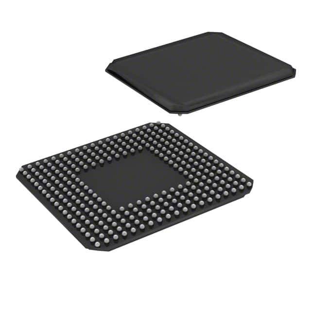
The XC95288XV-7CS280C is available in a CS280 package.
Essence
The essence of this product lies in its ability to provide reconfigurable logic functionality, allowing designers to create custom digital circuits without the need for dedicated hardware.
Packaging/Quantity
The XC95288XV-7CS280C is typically packaged individually and is available in various quantities depending on the supplier.
Specifications
- Logic Cells: 288
- Maximum Frequency: 100 MHz
- Operating Voltage: 3.3V
- I/O Pins: 208
- Package Type: CS280
Detailed Pin Configuration
The XC95288XV-7CS280C has a total of 208 I/O pins. These pins are organized into different banks, each serving a specific purpose. The pin configuration is as follows:
- Bank A: Pins 1-32
- Bank B: Pins 33-64
- Bank C: Pins 65-96
- Bank D: Pins 97-128
- Bank E: Pins 129-160
- Bank F: Pins 161-192
- Bank G: Pins 193-208
Functional Features
The XC95288XV-7CS280C offers several functional features that make it a versatile choice for digital circuit design:
- Reconfigurable Logic: The device can be programmed to implement various logic functions, allowing for flexibility in circuit design.
- Embedded Memory: It includes built-in memory blocks that can be used to store data or program code.
- Clock Management: The PLD provides dedicated clock resources for efficient timing control.
- I/O Flexibility: With a large number of I/O pins, the XC95288XV-7CS280C supports diverse interfacing requirements.
Advantages and Disadvantages
Advantages
- Versatility: The reconfigurable nature of this PLD allows for easy adaptation to changing design requirements.
- High Density: The XC95288XV-7CS280C offers a large number of logic cells, enabling complex designs to be implemented.
- Low Power Consumption: The device operates efficiently, minimizing power consumption.
Disadvantages
- Learning Curve: Utilizing the full potential of this PLD may require a learning curve for designers unfamiliar with programmable logic devices.
- Cost: Compared to fixed-function integrated circuits, PLDs can be relatively more expensive.
Working Principles
The XC95288XV-7CS280C operates based on the principles of field-programmable gate arrays (FPGAs). It consists of an array of configurable logic blocks interconnected by programmable routing resources. These logic blocks can be configured to perform specific functions using a hardware description language (HDL) or a graphical design tool. Once programmed, the PLD executes the desired logic operations.
Detailed Application Field Plans
The XC95288XV-7CS280C finds applications in various fields, including:
- Communications: It can be used in the design of communication systems, such as network routers and switches.
- Industrial Automation: The PLD is suitable for implementing control systems in industrial automation, enabling precise and efficient operation.
- Automotive Electronics: It can be utilized in automotive electronics for functions like engine control units (ECUs) and advanced driver-assistance systems (ADAS).
- Consumer Electronics: The XC95288XV-7CS280C can be employed in consumer electronic devices, such as gaming consoles and multimedia systems.
Detailed and Complete Alternative Models
- XC95144XL-10TQG100C: This alternative model offers similar functionality with 144 logic cells and a maximum frequency of 10 MHz.
- XC9536XL-10VQG44C: With 36 logic cells and a maximum frequency of 10 MHz, this alternative model is suitable for smaller-scale designs.
- XC9572XL-10VQG44C: This model provides 72 logic cells and a maximum frequency of 10 MHz, offering a balance between
Lista 10 Vanliga frågor och svar relaterade till tillämpningen av XC95288XV-7CS280C i tekniska lösningar
Sure! Here are 10 common questions and answers related to the application of XC95288XV-7CS280C in technical solutions:
Q: What is XC95288XV-7CS280C? A: XC95288XV-7CS280C is a specific model of Field Programmable Gate Array (FPGA) manufactured by Xilinx.
Q: What are the key features of XC95288XV-7CS280C? A: Some key features of XC95288XV-7CS280C include 288 macrocells, 280-pin package, 7ns maximum propagation delay, and 3.3V power supply.
Q: What are the typical applications of XC95288XV-7CS280C? A: XC95288XV-7CS280C is commonly used in various technical solutions such as digital signal processing, telecommunications, industrial automation, and embedded systems.
Q: How can I program XC95288XV-7CS280C? A: XC95288XV-7CS280C can be programmed using Xilinx's programming tools like iMPACT or Vivado, which allow you to configure the FPGA with your desired logic design.
Q: Can XC95288XV-7CS280C be reprogrammed after initial configuration? A: Yes, XC95288XV-7CS280C is a reprogrammable FPGA, meaning you can modify and reconfigure its logic design multiple times as per your requirements.
Q: What is the maximum operating frequency of XC95288XV-7CS280C? A: The maximum operating frequency of XC95288XV-7CS280C depends on the specific design and implementation, but it can typically reach frequencies in the range of tens to hundreds of megahertz.
Q: Can XC95288XV-7CS280C interface with other components or devices? A: Yes, XC95288XV-7CS280C supports various standard interfaces like GPIO (General Purpose Input/Output), SPI (Serial Peripheral Interface), I2C (Inter-Integrated Circuit), UART (Universal Asynchronous Receiver-Transmitter), etc., allowing it to communicate with other components or devices.
Q: What are the power requirements for XC95288XV-7CS280C? A: XC95288XV-7CS280C operates on a 3.3V power supply and consumes power based on its configuration and utilization.
Q: Are there any development boards available for XC95288XV-7CS280C? A: Yes, Xilinx provides development boards like the Xilinx Spartan-6 FPGA SP605 Evaluation Kit, which includes XC95288XV-7CS280C and allows you to prototype and test your designs.
Q: Where can I find more information about XC95288XV-7CS280C? A: You can refer to the official documentation and datasheets provided by Xilinx for detailed technical information about XC95288XV-7CS280C. Additionally, online forums and communities dedicated to FPGA programming can also be helpful sources of information.