

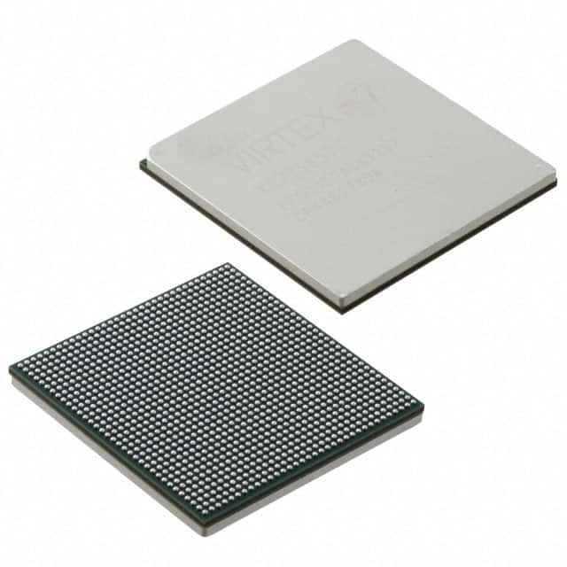
XC7VX690T-L2FFG1157E
Product Overview
Category
The XC7VX690T-L2FFG1157E belongs to the category of Field-Programmable Gate Arrays (FPGAs).
Use
FPGAs are integrated circuits that can be programmed and reprogrammed to perform various digital functions. The XC7VX690T-L2FFG1157E is specifically designed for high-performance applications that require complex logic and processing capabilities.
Characteristics
- High-performance FPGA with advanced features
- Large capacity and high-speed processing capabilities
- Flexible and reconfigurable design
- Supports a wide range of interfaces and protocols
- Optimized for power efficiency
Package
The XC7VX690T-L2FFG1157E comes in a compact and durable package, ensuring easy handling and protection during transportation and installation.
Essence
The essence of the XC7VX690T-L2FFG1157E lies in its ability to provide a customizable hardware platform for implementing complex digital systems. It offers designers the flexibility to create tailored solutions for a variety of applications.
Packaging/Quantity
The XC7VX690T-L2FFG1157E is typically packaged individually and is available in various quantities depending on the requirements of the customer.
Specifications
- Logic Cells: 1,006,080
- DSP Slices: 3,600
- Block RAM: 68,160 Kb
- Maximum I/Os: 1,157
- Operating Voltage: 1.0V
- Operating Temperature Range: -40°C to 100°C
- Package Type: Flip-Chip Fine-Pitch BGA
- Package Pins: 1,157
Detailed Pin Configuration
The XC7VX690T-L2FFG1157E has a complex pin configuration with 1,157 pins. These pins are distributed across various functional blocks and interfaces, allowing for versatile connectivity and integration within a system.
For a detailed pin configuration diagram and description, please refer to the product datasheet or user manual provided by the manufacturer.
Functional Features
The XC7VX690T-L2FFG1157E offers several functional features that make it suitable for demanding applications:
- High-speed processing: The FPGA is capable of handling complex logic operations at high clock frequencies, enabling rapid data processing.
- Flexible I/O interfaces: It supports a wide range of communication protocols, including Ethernet, USB, PCIe, and more, facilitating seamless integration with other devices.
- Reconfigurability: The FPGA can be reprogrammed on-the-fly, allowing for dynamic changes in functionality without requiring hardware modifications.
- Advanced DSP capabilities: The integrated Digital Signal Processing (DSP) slices enable efficient implementation of algorithms for signal processing applications.
- Large memory capacity: The abundant Block RAM resources provide ample storage for data buffering and caching, enhancing overall system performance.
Advantages and Disadvantages
Advantages
- High-performance and flexibility for complex applications
- Wide range of supported interfaces and protocols
- Power-efficient design
- Reconfigurable nature allows for adaptability to changing requirements
Disadvantages
- Steep learning curve for inexperienced users
- Higher cost compared to traditional fixed-function integrated circuits
- Requires specialized tools and expertise for programming and debugging
Working Principles
The XC7VX690T-L2FFG1157E operates based on the principles of digital logic design. It consists of an array of configurable logic blocks interconnected through programmable routing resources. These logic blocks can be programmed to implement desired functions using Hardware Description Languages (HDLs) such as VHDL or Verilog.
Upon programming, the FPGA's internal configuration memory is loaded, defining the desired functionality of the circuit. The FPGA then operates by executing the programmed logic, processing input signals, and generating output signals based on the defined logic functions.
Detailed Application Field Plans
The XC7VX690T-L2FFG1157E finds applications in various fields that require high-performance digital processing capabilities. Some potential application areas include:
- Telecommunications: Implementing advanced signal processing algorithms for wireless communication systems.
- Aerospace and Defense: Designing complex radar and communication systems for military applications.
- High-performance Computing: Accelerating computationally intensive tasks in scientific research and data analysis.
- Industrial Automation: Developing custom control systems for industrial machinery and robotics.
- Video and Image Processing: Real-time video encoding/decoding, image recognition, and computer vision applications.
Alternative Models
For users seeking alternative options, several other FPGA models with similar capabilities are available in the market. Some notable alternatives to the XC7VX690T-L2FFG1157E include:
- Xilinx Virtex-7 Series FPGAs
- Intel Stratix 10 FPGAs
- Lattice ECP5 FPGAs
Lista 10 Vanliga frågor och svar relaterade till tillämpningen av XC7VX690T-L2FFG1157E i tekniska lösningar
Question: What is the XC7VX690T-L2FFG1157E?
Answer: The XC7VX690T-L2FFG1157E is a high-performance field-programmable gate array (FPGA) manufactured by Xilinx.Question: What are the key features of the XC7VX690T-L2FFG1157E?
Answer: Some key features of this FPGA include a large number of programmable logic cells, high-speed transceivers, integrated memory blocks, and advanced DSP capabilities.Question: What are the typical applications for the XC7VX690T-L2FFG1157E?
Answer: This FPGA is commonly used in applications such as telecommunications, aerospace, defense, high-performance computing, and video processing.Question: How many logic cells does the XC7VX690T-L2FFG1157E have?
Answer: The XC7VX690T-L2FFG1157E has approximately 690,000 logic cells, making it suitable for complex designs.Question: Can I interface the XC7VX690T-L2FFG1157E with external devices?
Answer: Yes, this FPGA has a variety of I/O interfaces, including high-speed transceivers, LVDS, DDR3/DDR4 memory interfaces, and general-purpose I/O pins.Question: What is the power consumption of the XC7VX690T-L2FFG1157E?
Answer: The power consumption of this FPGA depends on the specific design and operating conditions. It is recommended to refer to the datasheet for detailed power specifications.Question: Can I reprogram the XC7VX690T-L2FFG1157E after it has been deployed in a system?
Answer: Yes, FPGAs are designed to be reprogrammable, allowing for flexibility and updates to the design even after deployment.Question: Are there any development tools available for programming the XC7VX690T-L2FFG1157E?
Answer: Yes, Xilinx provides a suite of development tools, including Vivado Design Suite, which allows designers to create, simulate, and program the FPGA.Question: What is the maximum operating frequency of the XC7VX690T-L2FFG1157E?
Answer: The maximum operating frequency of this FPGA depends on the specific design and implementation. It is recommended to refer to the datasheet for detailed timing specifications.Question: Can I use multiple XC7VX690T-L2FFG1157E FPGAs together in a system?
Answer: Yes, it is possible to use multiple FPGAs in a system to increase processing power or implement distributed computing architectures.