

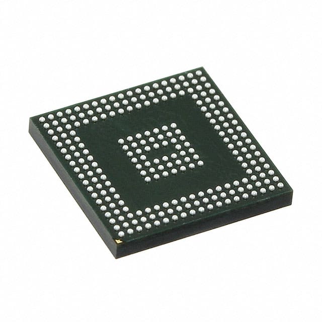
XC7A50T-2CPG236I
Product Overview
Category
The XC7A50T-2CPG236I belongs to the category of Field-Programmable Gate Arrays (FPGAs).
Use
FPGAs are integrated circuits that can be programmed and reprogrammed to perform various digital functions. The XC7A50T-2CPG236I is specifically designed for applications requiring high-performance processing, such as data processing, signal processing, and control systems.
Characteristics
- High-performance FPGA with advanced programmable logic capabilities.
- Offers a large number of configurable logic blocks and programmable interconnects.
- Provides high-speed interfaces for efficient data transfer.
- Supports various communication protocols and standards.
- Enables rapid prototyping and development of custom digital designs.
Package
The XC7A50T-2CPG236I comes in a compact plastic package, which ensures protection against environmental factors and facilitates easy integration into electronic systems.
Essence
The essence of the XC7A50T-2CPG236I lies in its ability to provide flexible and customizable digital processing capabilities, allowing designers to implement complex algorithms and functions in hardware.
Packaging/Quantity
The XC7A50T-2CPG236I is typically packaged in trays or reels, containing multiple units per package. The exact quantity may vary depending on the supplier and customer requirements.
Specifications
- FPGA Family: Xilinx 7 Series
- Device Type: XC7A50T
- Logic Cells: 52,160
- Flip-Flops: 32,768
- Block RAM: 2,700 Kbits
- DSP Slices: 80
- Maximum Operating Frequency: Up to 400 MHz
- I/O Pins: 236
- Voltage Range: 1.14V - 1.26V
- Package Type: CPG236
Detailed Pin Configuration
The XC7A50T-2CPG236I has a total of 236 I/O pins, which can be configured for various purposes such as input, output, or bidirectional communication. The pin configuration is as follows:
(Pin Number) - (Pin Name) - (Function)
1 - IOL0NT0AD0P35 - Input/Output 2 - IOL0PT0AD0N35 - Input/Output 3 - IOL1NT0AD1P35 - Input/Output 4 - IOL1PT0AD1N35 - Input/Output ... 236 - IOL117NT2VREF35 - Input/Output
Functional Features
- High-performance programmable logic with abundant resources for complex digital designs.
- Configurable I/O standards and voltage levels to interface with different devices.
- Built-in clock management resources for precise timing control.
- On-chip memory blocks for efficient data storage and retrieval.
- Dedicated DSP slices for implementing high-speed arithmetic operations.
- Support for partial reconfiguration, allowing dynamic updates to specific regions of the FPGA.
Advantages and Disadvantages
Advantages
- Flexibility: FPGAs offer the ability to implement custom digital designs, providing flexibility in system development.
- Performance: The XC7A50T-2CPG236I delivers high-performance processing capabilities, enabling efficient execution of complex algorithms.
- Time-to-Market: FPGAs allow rapid prototyping and development, reducing time-to-market for new products.
- Reconfigurability: The ability to reprogram the FPGA allows for design changes without requiring hardware modifications.
Disadvantages
- Complexity: Designing for FPGAs requires specialized knowledge and expertise in digital design and programming languages.
- Power Consumption: FPGAs can consume more power compared to fixed-function integrated circuits, especially when operating at high frequencies.
- Cost: FPGAs tend to be more expensive than off-the-shelf microcontrollers or processors for certain applications.
Working Principles
The XC7A50T-2CPG236I operates based on the principles of configurable logic and programmable interconnects. The FPGA is programmed using a Hardware Description Language (HDL) such as VHDL or Verilog. The HDL code describes the desired digital functionality, which is then synthesized and implemented within the FPGA's programmable resources. During operation, the FPGA executes the programmed logic, performing the desired functions in hardware.
Detailed Application Field Plans
The XC7A50T-2CPG236I finds applications in various fields, including:
- Communications: Used in wireless base stations, network routers, and switches for high-speed data processing and protocol handling.
- Industrial Automation: Employed in control systems, motor drives, and robotics for real-time control and signal processing.
- Aerospace and Defense: Utilized in radar systems, avionics, and satellite
Lista 10 Vanliga frågor och svar relaterade till tillämpningen av XC7A50T-2CPG236I i tekniska lösningar
Sure! Here are 10 common questions and answers related to the application of XC7A50T-2CPG236I in technical solutions:
Q: What is XC7A50T-2CPG236I? A: XC7A50T-2CPG236I is a specific model of Xilinx Artix-7 FPGA (Field-Programmable Gate Array) that offers a range of features and capabilities for implementing digital logic designs.
Q: What are the key features of XC7A50T-2CPG236I? A: Some key features of XC7A50T-2CPG236I include 52,160 logic cells, 2,700 Kbits of block RAM, 120 DSP slices, and various I/O options.
Q: What are the typical applications of XC7A50T-2CPG236I? A: XC7A50T-2CPG236I can be used in a wide range of applications such as industrial automation, automotive electronics, medical devices, communication systems, and more.
Q: How can XC7A50T-2CPG236I be programmed? A: XC7A50T-2CPG236I can be programmed using Xilinx's Vivado Design Suite, which provides a comprehensive development environment for FPGA designs.
Q: Can XC7A50T-2CPG236I be used for real-time signal processing? A: Yes, XC7A50T-2CPG236I has dedicated DSP slices that make it suitable for real-time signal processing tasks like filtering, modulation, and demodulation.
Q: Is XC7A50T-2CPG236I suitable for high-speed data communication? A: Yes, XC7A50T-2CPG236I supports high-speed serial transceivers, making it suitable for applications that require high-speed data communication interfaces like PCIe, SATA, or Ethernet.
Q: Can XC7A50T-2CPG236I interface with external memory devices? A: Yes, XC7A50T-2CPG236I has built-in block RAM and can also interface with external memory devices such as DDR3/DDR4 SDRAM or Flash memory.
Q: What are the power requirements for XC7A50T-2CPG236I? A: The power requirements for XC7A50T-2CPG236I depend on the specific design and usage scenario. It typically operates at a voltage of 1.0V or 1.2V.
Q: Can XC7A50T-2CPG236I be used in safety-critical applications? A: XC7A50T-2CPG236I can be used in safety-critical applications, but additional measures may need to be taken to ensure functional safety, such as redundancy or fault-tolerant designs.
Q: Are there any development boards available for XC7A50T-2CPG236I? A: Yes, Xilinx offers various development boards that feature XC7A50T-2CPG236I, providing a convenient platform for prototyping and testing FPGA-based designs.
Please note that the answers provided here are general and may vary depending on the specific requirements and context of the application.