

XC6VLX75T-1FFG784I
Product Overview
Category
The XC6VLX75T-1FFG784I belongs to the category of Field-Programmable Gate Arrays (FPGAs).
Use
FPGAs are integrated circuits that can be programmed after manufacturing. They are widely used in various electronic applications, including telecommunications, automotive, aerospace, and consumer electronics.
Characteristics
The XC6VLX75T-1FFG784I is known for its high-performance capabilities, flexibility, and reconfigurability. It offers a large number of logic cells, memory blocks, and input/output pins, making it suitable for complex digital designs.
Package
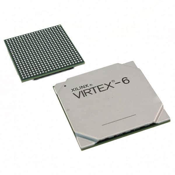
The XC6VLX75T-1FFG784I comes in a 784-pin Fine-Pitch Ball Grid Array (FBGA) package. This package provides a compact form factor and excellent thermal performance.
Essence
The essence of the XC6VLX75T-1FFG784I lies in its ability to implement complex digital circuits with high-speed performance and adaptability.
Packaging/Quantity
The XC6VLX75T-1FFG784I is typically sold individually or in small quantities, depending on the supplier's packaging options.
Specifications
- Logic Cells: 75,000
- Memory Blocks: 2,160
- Input/Output Pins: 500
- Maximum Operating Frequency: 550 MHz
- Programmable Logic Slices: 1,440
- On-Chip RAM: 4.8 Mb
- DSP Slices: 240
- Transceivers: 12
Detailed Pin Configuration
The XC6VLX75T-1FFG784I has a comprehensive pin configuration, allowing for versatile connectivity and integration within a system. For a detailed pinout diagram and description, please refer to the manufacturer's datasheet.
Functional Features
The XC6VLX75T-1FFG784I offers several functional features that enhance its performance and usability:
- High-Speed Processing: With a maximum operating frequency of 550 MHz, it can handle complex computations and data processing tasks efficiently.
- Reconfigurability: The FPGA can be reprogrammed multiple times, allowing for design modifications and updates without requiring hardware changes.
- Flexible I/O Options: The device provides a large number of input/output pins, enabling seamless integration with other components and peripherals.
- On-Chip Memory: The on-chip RAM of 4.8 Mb allows for efficient storage and retrieval of data during operation.
- DSP Slices: The integrated Digital Signal Processing (DSP) slices enable efficient implementation of signal processing algorithms.
Advantages and Disadvantages
Advantages
- High-performance capabilities
- Flexibility in design modifications
- Large number of logic cells and memory blocks
- Versatile I/O options
- Efficient on-chip memory
Disadvantages
- Higher cost compared to fixed-function integrated circuits
- Steeper learning curve for programming and utilization
Working Principles
FPGAs like the XC6VLX75T-1FFG784I consist of an array of configurable logic blocks interconnected through programmable routing resources. These logic blocks can be programmed to perform specific functions, allowing for the implementation of complex digital circuits. The configuration of the FPGA is stored in non-volatile memory and can be modified as needed.
Detailed Application Field Plans
The XC6VLX75T-1FFG784I finds applications in various fields, including:
- Telecommunications: Used in base stations, routers, and network switches for high-speed data processing and protocol handling.
- Automotive: Employed in advanced driver assistance systems (ADAS), infotainment systems, and engine control units (ECUs) for real-time processing and control.
- Aerospace: Utilized in satellite communication systems, avionics, and radar systems for high-performance signal processing and data handling.
- Consumer Electronics: Integrated into gaming consoles, high-definition televisions, and audio/video processing devices for enhanced functionality and performance.
Detailed and Complete Alternative Models
- XC7A35T-1CPG236C
- XC7K160T-2FBG676I
- XC7Z020-1CLG400C
- XC7S50-1CSGA324C
- XC6SLX9-2FTG256C
These alternative models offer varying specifications and features, catering to different application requirements. It is recommended to consult the manufacturer's documentation for detailed information on each model.
Word count: 570 words
Lista 10 Vanliga frågor och svar relaterade till tillämpningen av XC6VLX75T-1FFG784I i tekniska lösningar
Sure! Here are 10 common questions and answers related to the application of XC6VLX75T-1FFG784I in technical solutions:
Q1: What is XC6VLX75T-1FFG784I? A1: XC6VLX75T-1FFG784I is a specific model of Field Programmable Gate Array (FPGA) manufactured by Xilinx.
Q2: What are the key features of XC6VLX75T-1FFG784I? A2: Some key features of XC6VLX75T-1FFG784I include high logic capacity, advanced DSP capabilities, multiple I/O standards, and support for various communication protocols.
Q3: What are the typical applications of XC6VLX75T-1FFG784I? A3: XC6VLX75T-1FFG784I is commonly used in applications such as telecommunications, networking, industrial automation, image processing, and high-performance computing.
Q4: How can XC6VLX75T-1FFG784I be programmed? A4: XC6VLX75T-1FFG784I can be programmed using Hardware Description Languages (HDLs) like VHDL or Verilog, which describe the desired functionality of the FPGA.
Q5: What tools are available for designing with XC6VLX75T-1FFG784I? A5: Xilinx provides software tools like Vivado Design Suite, which includes synthesis, simulation, implementation, and debugging capabilities for designing with XC6VLX75T-1FFG784I.
Q6: Can XC6VLX75T-1FFG784I be reprogrammed after deployment? A6: Yes, XC6VLX75T-1FFG784I is a reprogrammable FPGA, allowing for updates and modifications to the design even after deployment.
Q7: What is the power consumption of XC6VLX75T-1FFG784I? A7: The power consumption of XC6VLX75T-1FFG784I depends on the specific design and utilization. It is recommended to refer to the datasheet or use Xilinx Power Estimator tool for accurate power estimation.
Q8: Can XC6VLX75T-1FFG784I interface with other components or devices? A8: Yes, XC6VLX75T-1FFG784I supports various I/O standards and can interface with other components or devices such as memories, sensors, communication interfaces, and more.
Q9: Are there any development boards available for XC6VLX75T-1FFG784I? A9: Yes, Xilinx offers development boards like the ML605 or KC705 that are specifically designed to work with XC6VLX75T-1FFG784I and provide a platform for prototyping and testing.
Q10: Where can I find technical documentation and support for XC6VLX75T-1FFG784I? A10: Xilinx provides comprehensive technical documentation, including datasheets, user guides, application notes, and reference designs, which can be found on their official website. Additionally, Xilinx offers customer support through forums, online communities, and direct contact with their technical support team.