

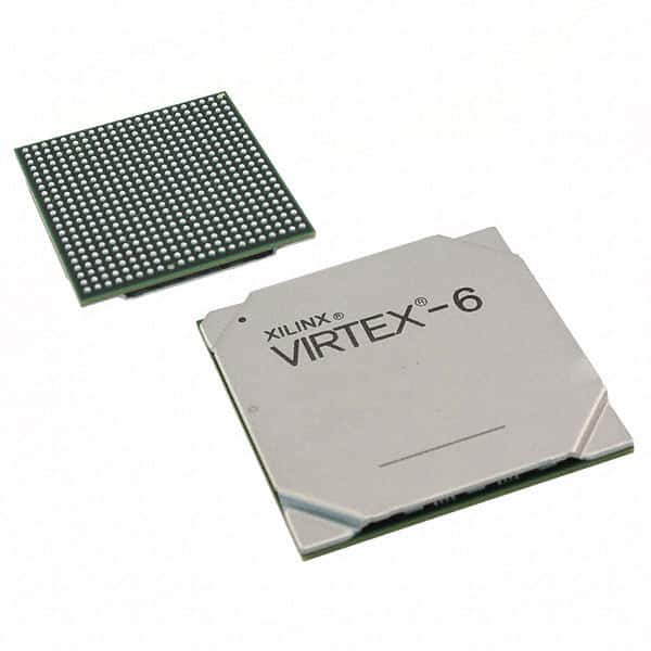
XC6VLX365T-L1FF1156I
Basic Information Overview
- Category: Field Programmable Gate Array (FPGA)
- Use: Digital logic circuits and systems design
- Characteristics:
- High-performance programmable logic device
- Large capacity and high-speed processing capabilities
- Flexible and reconfigurable architecture
- Package: Flip-chip BGA package
- Essence: Versatile and powerful FPGA for various applications
- Packaging/Quantity: Available in trays or reels, quantity depends on customer requirements
Specifications
- Logic Cells: 365,000
- Slices: 57,600
- DSP48E1 Slices: 728
- Block RAM: 4,860 Kb
- Maximum I/O Pins: 1,156
- Operating Voltage: 1.2V
- Speed Grade: L1FF
Detailed Pin Configuration
The XC6VLX365T-L1FF1156I has a total of 1,156 I/O pins, which are configurable based on the specific application requirements. The pin configuration includes input/output pins, clock pins, power supply pins, and configuration pins. The detailed pinout can be found in the manufacturer's datasheet.
Functional Features
- High-performance FPGA with advanced architecture
- Configurable logic cells for implementing complex digital designs
- Dedicated DSP slices for efficient signal processing
- On-chip memory blocks for data storage and retrieval
- Flexible I/O interfaces for connecting to external devices
- Built-in configuration interface for easy programming
Advantages and Disadvantages
Advantages: - Versatility: Can be used in a wide range of applications - Reconfigurability: Allows for quick design iterations and updates - High-performance: Capable of handling complex computations - Scalability: Supports designs of varying sizes and complexities
Disadvantages: - Cost: FPGAs can be more expensive compared to other programmable logic devices - Power Consumption: High-performance FPGAs may consume more power - Design Complexity: Requires expertise in digital design and FPGA programming
Working Principles
The XC6VLX365T-L1FF1156I is based on the concept of field-programmable gate arrays. It consists of a large number of configurable logic cells interconnected through programmable routing resources. These logic cells can be programmed to implement various digital functions, allowing designers to create custom digital circuits.
The FPGA's configuration is stored in non-volatile memory and loaded during startup. Once configured, the FPGA operates based on the programmed logic, performing the desired functions. The reconfigurability of FPGAs enables designers to modify or update the functionality without changing the hardware.
Detailed Application Field Plans
The XC6VLX365T-L1FF1156I finds applications in various fields, including: - Telecommunications: Implementing high-speed data processing and protocol handling. - Aerospace and Defense: Designing complex signal processing systems and radar applications. - Industrial Automation: Controlling and monitoring industrial processes with real-time capabilities. - Medical Devices: Developing advanced imaging and diagnostic equipment. - Research and Development: Prototyping and testing new digital designs.
Detailed and Complete Alternative Models
- XC6VLX75T-L1FF484I: Smaller capacity FPGA with 75,000 logic cells and 484 I/O pins.
- XC6VLX240T-L1FF1156I: Larger capacity FPGA with 240,000 logic cells and 1,156 I/O pins.
- XC6VLX550T-L1FF1759I: Higher performance FPGA with 550,000 logic cells and 1,759 I/O pins.
These alternative models offer different capacities and pin configurations to suit specific project requirements.
Word count: 511 words
Lista 10 Vanliga frågor och svar relaterade till tillämpningen av XC6VLX365T-L1FF1156I i tekniska lösningar
Sure! Here are 10 common questions and answers related to the application of XC6VLX365T-L1FF1156I in technical solutions:
Q1: What is XC6VLX365T-L1FF1156I? A1: XC6VLX365T-L1FF1156I is a specific model of Xilinx Virtex-6 FPGA (Field-Programmable Gate Array) that offers high-performance processing capabilities for various technical applications.
Q2: What are the key features of XC6VLX365T-L1FF1156I? A2: Some key features of XC6VLX365T-L1FF1156I include a large number of logic cells, high-speed serial transceivers, embedded memory blocks, DSP slices, and support for various communication protocols.
Q3: What are the typical applications of XC6VLX365T-L1FF1156I? A3: XC6VLX365T-L1FF1156I can be used in a wide range of applications such as telecommunications, aerospace, defense, industrial automation, medical imaging, and scientific research.
Q4: How can XC6VLX365T-L1FF1156I be programmed? A4: XC6VLX365T-L1FF1156I can be programmed using Xilinx's Vivado Design Suite or ISE Design Suite, which provide tools for designing, simulating, synthesizing, and implementing FPGA designs.
Q5: What is the power consumption of XC6VLX365T-L1FF1156I? A5: The power consumption of XC6VLX365T-L1FF1156I depends on the specific design and operating conditions. It is recommended to refer to the datasheet or use Xilinx's power estimation tools for accurate power consumption analysis.
Q6: Can XC6VLX365T-L1FF1156I be used for high-speed data processing? A6: Yes, XC6VLX365T-L1FF1156I is designed to handle high-speed data processing with its built-in high-speed serial transceivers and advanced DSP slices.
Q7: Does XC6VLX365T-L1FF1156I support different communication protocols? A7: Yes, XC6VLX365T-L1FF1156I supports various communication protocols such as PCIe, Ethernet, USB, SATA, and more, making it suitable for applications requiring connectivity.
Q8: Can XC6VLX365T-L1FF1156I be used in safety-critical applications? A8: Yes, XC6VLX365T-L1FF1156I can be used in safety-critical applications. However, additional design considerations and validation processes may be required to meet the specific safety standards of the application.
Q9: What are the temperature and operating conditions for XC6VLX365T-L1FF1156I? A9: The recommended operating temperature range for XC6VLX365T-L1FF1156I is typically -40°C to +100°C. It is important to refer to the datasheet for detailed information on operating conditions.
Q10: Are there any development boards or evaluation kits available for XC6VLX365T-L1FF1156I? A10: Yes, Xilinx offers development boards and evaluation kits that include XC6VLX365T-L1FF1156I, allowing users to prototype and test their designs before production.
Please note that the answers provided here are general and may vary depending on specific requirements and design considerations. It is always recommended to refer to the official documentation and consult with Xilinx or technical experts for accurate and up-to-date information.