

XC3S400A-4FG400I
Product Overview
Category
The XC3S400A-4FG400I belongs to the category of Field Programmable Gate Arrays (FPGAs).
Use
FPGAs are integrated circuits that can be programmed and reprogrammed to perform various digital functions. The XC3S400A-4FG400I is specifically designed for applications requiring high-performance logic capacity and flexibility.
Characteristics
- High-performance FPGA with 400,000 system gates
- Low power consumption
- Fast configuration and reconfiguration times
- Wide range of I/O options
- Support for various communication protocols
- Built-in memory blocks for efficient data storage
Package
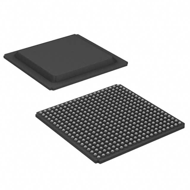
The XC3S400A-4FG400I comes in a FG400 package, which refers to a fine-pitch ball grid array (BGA) package with 400 pins.
Essence
The essence of the XC3S400A-4FG400I lies in its ability to provide a customizable hardware platform for implementing complex digital designs. It offers a high level of integration and flexibility, making it suitable for a wide range of applications.
Packaging/Quantity
The XC3S400A-4FG400I is typically packaged individually and is available in various quantities depending on the manufacturer's specifications.
Specifications
- Logic Cells: 400,000
- System Gates: 400,000
- Block RAM: 1,728 Kbits
- DSP Slices: 192
- Maximum I/O Pins: 317
- Operating Voltage: 1.2V
- Operating Temperature Range: -40°C to 100°C
Detailed Pin Configuration
The XC3S400A-4FG400I has a total of 400 pins arranged in a fine-pitch ball grid array (BGA) package. The pin configuration includes dedicated input/output pins, power supply pins, ground pins, and configuration pins. A detailed pinout diagram can be found in the product datasheet.
Functional Features
- High logic capacity for complex designs
- Flexible and reprogrammable architecture
- Support for various communication protocols (e.g., SPI, I2C)
- Built-in memory blocks for efficient data storage
- Low power consumption for energy-efficient applications
- Fast configuration and reconfiguration times for quick prototyping and development
Advantages and Disadvantages
Advantages
- High-performance FPGA with a large number of logic cells
- Flexibility to implement complex digital designs
- Support for various communication protocols
- Efficient use of resources with built-in memory blocks
- Low power consumption for energy-efficient applications
Disadvantages
- Fine-pitch BGA package may require specialized assembly techniques
- Limited availability of alternative models with similar specifications
Working Principles
The XC3S400A-4FG400I operates based on the principles of field-programmable gate arrays. It consists of an array of configurable logic blocks (CLBs) interconnected through programmable routing resources. The device can be programmed using hardware description languages (HDLs) or graphical tools to define the desired digital circuit functionality. Once programmed, the FPGA can execute the specified logic operations.
Detailed Application Field Plans
The XC3S400A-4FG400I finds applications in various fields, including:
- Telecommunications: Used in base stations, network switches, and routers for high-speed data processing and protocol handling.
- Industrial Automation: Employed in control systems, motor drives, and robotics for real-time control and signal processing.
- Aerospace and Defense: Utilized in radar systems, avionics, and military communication equipment for high-performance signal processing and encryption.
- Medical Devices: Integrated into medical imaging systems, patient monitoring devices, and laboratory equipment for data acquisition and processing.
- Automotive: Used in advanced driver-assistance systems (ADAS), infotainment systems, and engine control units (ECUs) for enhanced functionality and performance.
Detailed and Complete Alternative Models
While the XC3S400A-4FG400I offers a unique combination of features and specifications, there are alternative models available from other FPGA manufacturers. Some notable alternatives include:
- Altera Cyclone IV EP4CE40F23C8N
- Lattice Semiconductor iCE40HX1K-TQ144
- Xilinx Spartan-6 XC6SLX9-2TQG144C
These alternative models offer similar capabilities and can be considered based on specific project requirements and cost considerations.
In conclusion, the XC3S400A-4FG400I is a high-performance FPGA that provides flexibility, scalability, and integration for various digital design applications. Its extensive logic capacity, low power consumption, and support for multiple communication protocols make it a versatile choice for designers seeking customizable hardware solutions.
Lista 10 Vanliga frågor och svar relaterade till tillämpningen av XC3S400A-4FG400I i tekniska lösningar
Sure! Here are 10 common questions and answers related to the application of XC3S400A-4FG400I in technical solutions:
Q: What is XC3S400A-4FG400I? A: XC3S400A-4FG400I is a field-programmable gate array (FPGA) from Xilinx, which offers programmable logic and digital signal processing capabilities.
Q: What are the key features of XC3S400A-4FG400I? A: Some key features include 400,000 system gates, 400 I/O pins, 4-input look-up tables, built-in multipliers, and high-speed serial interfaces.
Q: What are the typical applications of XC3S400A-4FG400I? A: XC3S400A-4FG400I is commonly used in various applications such as industrial automation, telecommunications, automotive electronics, medical devices, and aerospace systems.
Q: How can XC3S400A-4FG400I be programmed? A: XC3S400A-4FG400I can be programmed using Xilinx's Vivado Design Suite or ISE Design Suite software tools, which allow users to design and implement their custom logic circuits.
Q: Can XC3S400A-4FG400I interface with other components or devices? A: Yes, XC3S400A-4FG400I supports various standard interfaces like SPI, I2C, UART, Ethernet, and PCIe, enabling seamless integration with other components or devices.
Q: What are the power requirements for XC3S400A-4FG400I? A: XC3S400A-4FG400I typically operates at a voltage range of 1.14V to 1.26V, with a maximum power consumption of around 2W.
Q: Can XC3S400A-4FG400I be reprogrammed multiple times? A: Yes, XC3S400A-4FG400I is a reprogrammable FPGA, allowing users to modify and reconfigure the logic design multiple times as per their requirements.
Q: Are there any development boards available for XC3S400A-4FG400I? A: Yes, Xilinx offers development boards like the Spartan-3A Evaluation Kit, which provide a platform for prototyping and testing designs using XC3S400A-4FG400I.
Q: What kind of support is available for XC3S400A-4FG400I? A: Xilinx provides comprehensive technical documentation, application notes, reference designs, and an active online community to support users working with XC3S400A-4FG400I.
Q: Can XC3S400A-4FG400I be used in safety-critical applications? A: Yes, XC3S400A-4FG400I can be used in safety-critical applications, but it requires proper design considerations, validation, and adherence to relevant safety standards.
Please note that these answers are general and may vary depending on specific use cases and requirements.