

XC3S1000-4FGG320I
Product Overview
Category
XC3S1000-4FGG320I belongs to the category of Field Programmable Gate Arrays (FPGAs).
Use
FPGAs are integrated circuits that can be programmed and reprogrammed to perform various digital functions. They are widely used in industries such as telecommunications, automotive, aerospace, and consumer electronics.
Characteristics
- High flexibility: FPGAs can be customized to perform specific tasks by programming the logic gates and interconnections.
- Parallel processing: FPGAs can execute multiple operations simultaneously, making them suitable for applications requiring high-speed data processing.
- Reconfigurability: FPGAs can be reprogrammed multiple times, allowing for design changes or updates without replacing the hardware.
- Low power consumption: Compared to traditional application-specific integrated circuits (ASICs), FPGAs consume less power.
Package and Quantity
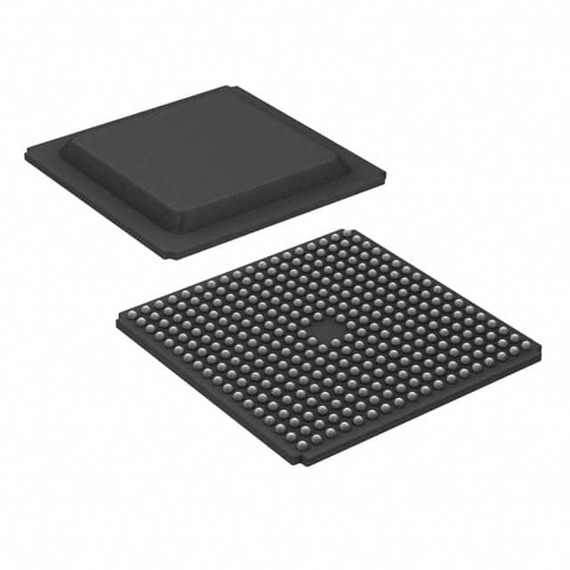
XC3S1000-4FGG320I is available in a Fine-Pitch Ball Grid Array (FBGA) package. The quantity per package may vary depending on the supplier.
Specifications
- Model: XC3S1000-4FGG320I
- Logic Cells: 1,000
- Maximum Frequency: 400 MHz
- Operating Voltage: 1.2V
- I/O Pins: 320
- Memory Blocks: 36
- Embedded Multiplier Blocks: 4
Pin Configuration
The detailed pin configuration of XC3S1000-4FGG320I can be found in the product datasheet provided by the manufacturer.
Functional Features
- Programmable Logic: The FPGA can be configured to implement various logical functions, enabling complex digital designs.
- Memory Integration: The embedded memory blocks allow for efficient storage and retrieval of data within the FPGA.
- Clock Management: The device supports advanced clocking features, including phase-locked loops (PLLs) for precise timing control.
- I/O Flexibility: The FPGA provides a large number of I/O pins, allowing for versatile interfacing with external devices.
Advantages
- Versatility: FPGAs offer the flexibility to adapt to changing requirements and can be reprogrammed as needed.
- Rapid Prototyping: FPGAs enable quick development and testing of digital designs, reducing time-to-market.
- Cost-Effective: Compared to ASICs, FPGAs have lower upfront costs and can be manufactured in smaller quantities.
- High Performance: FPGAs can achieve high-speed data processing and parallel execution of tasks.
Disadvantages
- Power Consumption: FPGAs generally consume more power compared to dedicated hardware solutions.
- Complexity: Designing and programming FPGAs require specialized knowledge and expertise.
- Limited Resources: The available logic cells, memory blocks, and I/O pins may impose constraints on complex designs.
Working Principles
FPGAs consist of an array of configurable logic blocks interconnected by programmable interconnects. The logic blocks contain look-up tables (LUTs), flip-flops, and other components that can be programmed to implement desired logic functions. The interconnects allow for routing signals between different blocks, enabling communication and data flow within the FPGA.
Application Field Plans
XC3S1000-4FGG320I finds applications in various fields, including: 1. Telecommunications: FPGAs are used in network routers, switches, and base stations for high-speed data processing and protocol handling. 2. Automotive: FPGAs are employed in automotive electronics for functions like engine control, driver assistance systems, and infotainment. 3. Aerospace: FPGAs are utilized in satellite communication systems, avionics, and radar systems for their reliability and performance. 4. Consumer Electronics: FPGAs are integrated into devices like high-definition televisions, gaming consoles, and digital cameras for enhanced functionality.
Alternative Models
Other FPGA models that can be considered as alternatives to XC3S1000-4FGG320I include: - Xilinx Spartan-6 XC6SLX9 - Altera Cyclone IV EP4CE6 - Lattice iCE40HX1K
These alternative models offer different specifications and features, allowing designers to choose the most suitable FPGA for their specific application requirements.
In conclusion, XC3S1000-4FGG320I is a versatile FPGA with high flexibility, reconfigurability, and parallel processing capabilities. It finds applications in various industries and offers advantages such as rapid prototyping and cost-effectiveness. However, it also has limitations in terms of power consumption and design complexity. Understanding its working principles and considering alternative models can help engineers make informed decisions when utilizing FPGAs in their designs.
Lista 10 Vanliga frågor och svar relaterade till tillämpningen av XC3S1000-4FGG320I i tekniska lösningar
Sure! Here are 10 common questions and answers related to the application of XC3S1000-4FGG320I in technical solutions:
Q: What is XC3S1000-4FGG320I? A: XC3S1000-4FGG320I is a field-programmable gate array (FPGA) manufactured by Xilinx. It is part of the Spartan-3 family and has 1000 logic cells.
Q: What are the key features of XC3S1000-4FGG320I? A: Some key features include 1000 logic cells, 32 I/O pins, 4-input look-up tables, 18-bit block RAMs, and a maximum operating frequency of 200 MHz.
Q: What are the typical applications of XC3S1000-4FGG320I? A: XC3S1000-4FGG320I can be used in various applications such as digital signal processing, embedded systems, industrial automation, telecommunications, and high-performance computing.
Q: How do I program XC3S1000-4FGG320I? A: XC3S1000-4FGG320I can be programmed using Xilinx's Vivado or ISE Design Suite software. You can write your design in a hardware description language (HDL) like VHDL or Verilog and then synthesize, implement, and generate a bitstream file for programming the FPGA.
Q: Can XC3S1000-4FGG320I be reprogrammed? A: Yes, XC3S1000-4FGG320I is a reprogrammable FPGA. You can erase the existing configuration and program it with a new design multiple times.
Q: What is the power supply requirement for XC3S1000-4FGG320I? A: The recommended operating voltage for XC3S1000-4FGG320I is 1.14V to 1.26V. It also requires a separate 2.5V auxiliary supply for configuration.
Q: Can XC3S1000-4FGG320I interface with other components or devices? A: Yes, XC3S1000-4FGG320I has various I/O pins that can be used to interface with other components or devices such as sensors, displays, memory modules, and communication interfaces.
Q: What are the available development boards or evaluation kits for XC3S1000-4FGG320I? A: Xilinx provides development boards like the Spartan-3E Starter Kit and the Nexys 2 board, which can be used for prototyping and testing designs based on XC3S1000-4FGG320I.
Q: Are there any limitations or constraints to consider when using XC3S1000-4FGG320I? A: Some limitations include limited logic resources compared to higher-end FPGAs, limited number of I/O pins, and lower maximum operating frequency compared to newer FPGA families.
Q: Where can I find more information or support for XC3S1000-4FGG320I? A: You can refer to the official Xilinx website for datasheets, user guides, application notes, and technical support related to XC3S1000-4FGG320I. Additionally, online forums and communities dedicated to FPGA development can provide valuable insights and assistance.