

XC2V1000-5FGG456C
Product Overview
Category
XC2V1000-5FGG456C belongs to the category of Field Programmable Gate Arrays (FPGAs).
Use
This FPGA is primarily used for digital logic design and implementation in various electronic systems.
Characteristics
- High-performance programmable logic device
- Offers flexibility and reconfigurability
- Enables rapid prototyping and development of complex digital circuits
- Supports a wide range of applications
Package
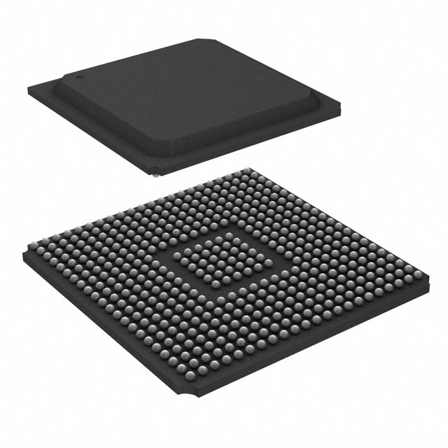
XC2V1000-5FGG456C comes in a Fine-Pitch Ball Grid Array (FBGA) package.
Essence
The essence of XC2V1000-5FGG456C lies in its ability to provide a customizable hardware platform for implementing digital designs.
Packaging/Quantity
XC2V1000-5FGG456C is typically packaged individually and is available in varying quantities depending on customer requirements.
Specifications
- Device Type: FPGA
- Family: Virtex-II
- Logic Cells: 1,000
- Speed Grade: -5
- Package Type: FBGA
- Package Pins: 456
- Operating Voltage: 3.3V
- Maximum Frequency: 200 MHz
- I/O Standards: LVCMOS, LVTTL, HSTL, SSTL, LVDS, etc.
- Configuration: SRAM-based
Detailed Pin Configuration
The detailed pin configuration of XC2V1000-5FGG456C can be found in the product datasheet provided by the manufacturer.
Functional Features
- High-density programmable logic cells
- Flexible interconnect resources
- Dedicated DSP slices for efficient signal processing
- Block RAM for data storage
- Clock management resources for precise timing control
- Built-in configuration memory for easy reprogramming
Advantages and Disadvantages
Advantages
- Versatile and adaptable for a wide range of applications
- Rapid prototyping and development capabilities
- High-performance and efficient logic implementation
- Reconfigurable nature allows for design iterations and updates
Disadvantages
- Higher cost compared to fixed-function integrated circuits
- Steeper learning curve for programming and utilization
- Limited resources may restrict the complexity of designs
Working Principles
XC2V1000-5FGG456C operates based on the principles of configurable logic blocks, interconnect resources, and programmable routing. The FPGA can be programmed using Hardware Description Languages (HDLs) such as VHDL or Verilog. The configuration data is stored in the internal memory of the device and can be modified as required.
Detailed Application Field Plans
XC2V1000-5FGG456C finds applications in various fields, including: - Digital signal processing - Communication systems - Embedded systems - Industrial automation - Aerospace and defense - Medical devices - Research and development
Detailed and Complete Alternative Models
Some alternative models to XC2V1000-5FGG456C include: - XC2V2000-4FF896C - XC2V3000-6FF1152C - XC2V4000-7FF1704C - XC2V6000-8FF1920C
These alternative models offer varying capacities, pin counts, and performance levels to cater to different project requirements.
Word count: 410 words
Lista 10 Vanliga frågor och svar relaterade till tillämpningen av XC2V1000-5FGG456C i tekniska lösningar
Sure! Here are 10 common questions and answers related to the application of XC2V1000-5FGG456C in technical solutions:
Q: What is XC2V1000-5FGG456C? A: XC2V1000-5FGG456C is a field-programmable gate array (FPGA) manufactured by Xilinx. It is designed for high-performance applications and offers 1000 logic cells.
Q: What are the key features of XC2V1000-5FGG456C? A: Some key features of XC2V1000-5FGG456C include 1000 logic cells, 456-pin Fine-Pitch Ball Grid Array (FBGA) package, 5ns maximum pin-to-pin delay, and support for various I/O standards.
Q: What are the typical applications of XC2V1000-5FGG456C? A: XC2V1000-5FGG456C can be used in a wide range of applications such as digital signal processing, telecommunications, industrial control systems, aerospace, and defense.
Q: How can I program XC2V1000-5FGG456C? A: XC2V1000-5FGG456C can be programmed using Xilinx's Vivado Design Suite or ISE Design Suite software tools. These tools allow you to design, simulate, and program the FPGA.
Q: What voltage levels does XC2V1000-5FGG456C support? A: XC2V1000-5FGG456C supports both 3.3V and 2.5V power supply voltages. The I/O pins are compatible with various voltage standards such as LVCMOS, LVTTL, and LVDS.
Q: Can XC2V1000-5FGG456C be used in a multi-FPGA system? A: Yes, XC2V1000-5FGG456C can be used in a multi-FPGA system. It supports various communication interfaces like SPI, JTAG, and SelectMAP for inter-FPGA communication.
Q: What is the maximum operating frequency of XC2V1000-5FGG456C? A: The maximum operating frequency of XC2V1000-5FGG456C depends on the design and implementation. However, it can typically achieve frequencies in the range of tens to hundreds of megahertz.
Q: Does XC2V1000-5FGG456C have built-in memory? A: No, XC2V1000-5FGG456C does not have built-in memory. However, it has dedicated block RAMs that can be used for implementing memory elements in your design.
Q: Can XC2V1000-5FGG456C interface with external devices? A: Yes, XC2V1000-5FGG456C can interface with external devices using its I/O pins. It supports various protocols such as UART, SPI, I2C, and Ethernet.
Q: Are there any development boards available for XC2V1000-5FGG456C? A: Yes, Xilinx provides development boards like the Spartan-3E Starter Kit that can be used for prototyping and testing designs based on XC2V1000-5FGG456C.
Please note that the answers provided here are general and may vary depending on specific requirements and use cases.