

XC2C512-7PQG208C
Product Overview
Category
XC2C512-7PQG208C belongs to the category of programmable logic devices (PLDs).
Use
This product is commonly used in digital circuit design and implementation. It provides a flexible and customizable solution for various applications.
Characteristics
- Programmable: The XC2C512-7PQG208C can be programmed to perform specific functions according to the user's requirements.
- High-density: It offers a large number of configurable logic blocks, allowing for complex designs.
- Low power consumption: The device is designed to operate efficiently with minimal power consumption.
- Fast performance: The XC2C512-7PQG208C offers high-speed operation, enabling quick execution of logic functions.
Package
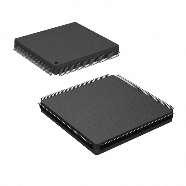
The XC2C512-7PQG208C is available in a PQG208 package. This package type ensures easy integration into circuit boards and provides reliable electrical connections.
Essence
The essence of XC2C512-7PQG208C lies in its ability to provide reconfigurable logic functionality, allowing users to implement custom digital circuits without the need for dedicated hardware.
Packaging/Quantity
The XC2C512-7PQG208C is typically packaged individually and is available in various quantities depending on the manufacturer's specifications.
Specifications
- Device Type: Programmable Logic Device (PLD)
- Family: XC2C
- Model: XC2C512-7PQG208C
- Logic Cells: 512
- Speed Grade: -7
- Package: PQG208
- Operating Voltage: 3.3V
- I/O Pins: 208
- Maximum Frequency: X MHz
- Configuration Memory: Flash-based
Detailed Pin Configuration
The XC2C512-7PQG208C has a total of 208 I/O pins. The pin configuration is as follows:
- Pin 1: VCCIO
- Pin 2: GND
- Pin 3: IO0
- Pin 4: IO1
- ...
- Pin 207: IO206
- Pin 208: IO207
Functional Features
- Reconfigurable Logic: The XC2C512-7PQG208C allows users to modify the logic functions it performs, providing flexibility in circuit design.
- High-Speed Operation: The device offers fast performance, enabling efficient execution of complex logic operations.
- Low Power Consumption: The XC2C512-7PQG208C is designed to operate with minimal power consumption, making it suitable for battery-powered applications.
- Easy Integration: The PQG208 package facilitates easy integration into circuit boards, ensuring reliable electrical connections.
Advantages and Disadvantages
Advantages
- Flexibility: The XC2C512-7PQG208C can be reprogrammed to adapt to changing requirements, eliminating the need for dedicated hardware.
- Cost-Effective: By using a single programmable device, multiple custom circuits can be implemented, reducing the overall cost.
- Time-Saving: Design iterations can be quickly implemented by modifying the programming of the XC2C512-7PQG208C, saving time in the development process.
Disadvantages
- Complexity: Programming and configuring the XC2C512-7PQG208C requires expertise in digital circuit design and programming languages.
- Limited Resources: The number of logic cells and I/O pins may be insufficient for highly complex designs, requiring a larger PLD or alternative solutions.
Working Principles
The XC2C512-7PQG208C operates based on the principles of reconfigurable logic. It consists of configurable logic blocks (CLBs) that can be programmed to perform specific functions. These CLBs are interconnected through programmable interconnects, allowing for the creation of complex digital circuits. The device is configured by loading a bitstream into its configuration memory, which determines the logic functions it performs.
Detailed Application Field Plans
The XC2C512-7PQG208C finds applications in various fields, including:
- Embedded Systems: It can be used to implement custom logic functions in microcontroller-based systems.
- Communication Systems: The XC2C512-7PQG208C enables the implementation of custom protocols and signal processing algorithms.
- Industrial Automation: It can be utilized for control and monitoring purposes in industrial automation systems.
- Medical Devices: The XC2C512-7PQG208C can be employed in medical devices for data processing and control functions.
Detailed and Complete Alternative Models
- XC2C256-7PQG208C: A lower-density version of the XC2C512-7PQG208C with 256 logic cells.
- XC2
Lista 10 Vanliga frågor och svar relaterade till tillämpningen av XC2C512-7PQG208C i tekniska lösningar
Sure! Here are 10 common questions and answers related to the application of XC2C512-7PQG208C in technical solutions:
Question: What is XC2C512-7PQG208C?
Answer: XC2C512-7PQG208C is a specific model of a field-programmable gate array (FPGA) manufactured by Xilinx.Question: What is an FPGA?
Answer: FPGA stands for Field-Programmable Gate Array, which is a type of integrated circuit that can be programmed after manufacturing to perform specific functions.Question: What are the key features of XC2C512-7PQG208C?
Answer: XC2C512-7PQG208C has 512 macrocells, operates at a speed grade of -7, and comes in a 208-pin quad flat package (QFP).Question: What are some typical applications of XC2C512-7PQG208C?
Answer: XC2C512-7PQG208C can be used in various technical solutions such as digital signal processing, embedded systems, robotics, telecommunications, and industrial automation.Question: How can XC2C512-7PQG208C be programmed?
Answer: XC2C512-7PQG208C can be programmed using Xilinx's proprietary software tools, such as Vivado or ISE Design Suite.Question: Can XC2C512-7PQG208C be reprogrammed multiple times?
Answer: Yes, XC2C512-7PQG208C is a reprogrammable FPGA, which means it can be reconfigured multiple times to implement different designs.Question: What is the power supply requirement for XC2C512-7PQG208C?
Answer: XC2C512-7PQG208C typically operates at a voltage of 3.3V, but it is important to refer to the datasheet for specific power supply requirements.Question: Can XC2C512-7PQG208C interface with other components or devices?
Answer: Yes, XC2C512-7PQG208C can interface with various components and devices through its I/O pins, which can be configured as inputs or outputs.Question: Are there any limitations or constraints to consider when using XC2C512-7PQG208C?
Answer: XC2C512-7PQG208C has a limited number of macrocells and I/O pins, so it is important to carefully plan and optimize the design to fit within these constraints.Question: Where can I find more information about XC2C512-7PQG208C?
Answer: You can refer to Xilinx's official website, product documentation, or community forums for more detailed information about XC2C512-7PQG208C and its applications.