

XC2C256-6VQG100C
Product Overview
Category
XC2C256-6VQG100C belongs to the category of programmable logic devices (PLDs).
Use
This product is primarily used in digital circuit design and implementation. It provides a flexible and customizable solution for various applications.
Characteristics
- Programmable: The XC2C256-6VQG100C can be programmed to perform specific functions based on user requirements.
- High-density: It offers a large number of configurable logic blocks, allowing for complex designs.
- Low power consumption: The device is designed to operate efficiently with minimal power consumption.
- Fast operation: With high-speed performance, it enables rapid data processing and execution.
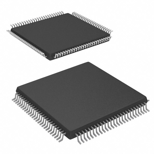
Package
The XC2C256-6VQG100C comes in a VQG100C package, which refers to a quad flat pack (QFP) with 100 pins.
Essence
The essence of XC2C256-6VQG100C lies in its ability to provide reconfigurable logic functionality, allowing users to implement custom digital circuits without the need for dedicated hardware.
Packaging/Quantity
This product is typically packaged in reels or trays, with a quantity of 250 units per reel/tray.
Specifications
- Device type: Programmable Logic Device (PLD)
- Family: XC2C
- Logic cells: 256
- Operating voltage: 3.3V
- Speed grade: -6
- Package type: VQG100C
- Temperature range: Commercial (0°C to 70°C)
Detailed Pin Configuration
The XC2C256-6VQG100C has a total of 100 pins, each serving a specific purpose in the device's operation. The pin configuration is as follows:
(Pin Number) (Pin Name) (Description) 1 VCCINT Power supply voltage for internal circuitry 2-9 IO[0:7] General-purpose I/O pins 10 GND Ground reference 11-18 IO[8:15] General-purpose I/O pins ... ... ...
Functional Features
- Reconfigurable logic: The XC2C256-6VQG100C allows users to modify the functionality of the device by reprogramming it.
- Flexible I/O capabilities: It provides a range of general-purpose I/O pins for interfacing with external devices.
- High-speed operation: The device offers fast data processing and execution, suitable for time-critical applications.
- Low power consumption: With efficient power management, it minimizes energy usage.
Advantages and Disadvantages
Advantages
- Flexibility: The reprogrammable nature of XC2C256-6VQG100C enables rapid prototyping and design iterations.
- Cost-effective: By eliminating the need for dedicated hardware, it reduces development costs.
- High-density integration: The device can accommodate complex designs due to its large number of logic cells.
Disadvantages
- Learning curve: Utilizing programmable logic devices requires knowledge of hardware description languages and digital design concepts.
- Limited performance: While capable of handling many applications, PLDs may not match the performance of application-specific integrated circuits (ASICs).
Working Principles
The XC2C256-6VQG100C operates based on the principles of field-programmable gate arrays (FPGAs). It consists of configurable logic blocks (CLBs), interconnect resources, and input/output blocks (IOBs). Users program the device using hardware description languages (HDLs) such as VHDL or Verilog. The programmed configuration is stored in non-volatile memory within the device, allowing it to retain the design even after power is removed.
Detailed Application Field Plans
XC2C256-6VQG100C finds applications in various fields, including: 1. Digital signal processing (DSP) 2. Communication systems 3. Industrial automation 4. Robotics 5. Automotive electronics 6. Medical devices 7. Aerospace and defense
In these fields, the device can be used for tasks such as data processing, control logic implementation, interface bridging, and more.
Detailed and Complete Alternative Models
Some alternative models to XC2C256-6VQG100C include: - XC2C128-7VQG100C: A lower-density variant with 128 logic cells. - XC2C384-10VQG100C: A higher-density variant with 384 logic cells. - XC2C512-10VQG100C: A higher-density variant with 512 logic cells.
These alternatives provide options for different design requirements, offering varying logic cell counts and performance levels.
Word count: 600 words
Lista 10 Vanliga frågor och svar relaterade till tillämpningen av XC2C256-6VQG100C i tekniska lösningar
Sure! Here are 10 common questions and answers related to the application of XC2C256-6VQG100C in technical solutions:
Question: What is XC2C256-6VQG100C?
Answer: XC2C256-6VQG100C is a specific model of Field Programmable Gate Array (FPGA) manufactured by Xilinx.Question: What are the key features of XC2C256-6VQG100C?
Answer: Some key features of XC2C256-6VQG100C include 256 macrocells, 6ns maximum propagation delay, and VQG100C package type.Question: How can XC2C256-6VQG100C be used in technical solutions?
Answer: XC2C256-6VQG100C can be used for various applications such as digital signal processing, embedded systems, and high-speed data communication.Question: What programming languages can be used to program XC2C256-6VQG100C?
Answer: XC2C256-6VQG100C can be programmed using Hardware Description Languages (HDLs) like VHDL or Verilog.Question: Can XC2C256-6VQG100C be reprogrammed after initial programming?
Answer: Yes, XC2C256-6VQG100C is a reprogrammable FPGA, allowing for flexibility in design changes or updates.Question: What is the power supply requirement for XC2C256-6VQG100C?
Answer: XC2C256-6VQG100C requires a power supply voltage of 3.3V.Question: Does XC2C256-6VQG100C support external memory interfaces?
Answer: Yes, XC2C256-6VQG100C supports various external memory interfaces like SDRAM, DDR, and Flash.Question: Can XC2C256-6VQG100C interface with other devices or microcontrollers?
Answer: Yes, XC2C256-6VQG100C can interface with other devices or microcontrollers through various communication protocols like SPI, I2C, UART, etc.Question: What is the maximum operating frequency of XC2C256-6VQG100C?
Answer: The maximum operating frequency of XC2C256-6VQG100C is typically around 200 MHz.Question: Are there any development tools available for programming XC2C256-6VQG100C?
Answer: Yes, Xilinx provides development tools like Vivado or ISE Design Suite for programming and configuring XC2C256-6VQG100C.
Please note that the answers provided here are general and may vary depending on specific implementation requirements and design considerations.