

2N6660JTVP02
Product Category: Transistor
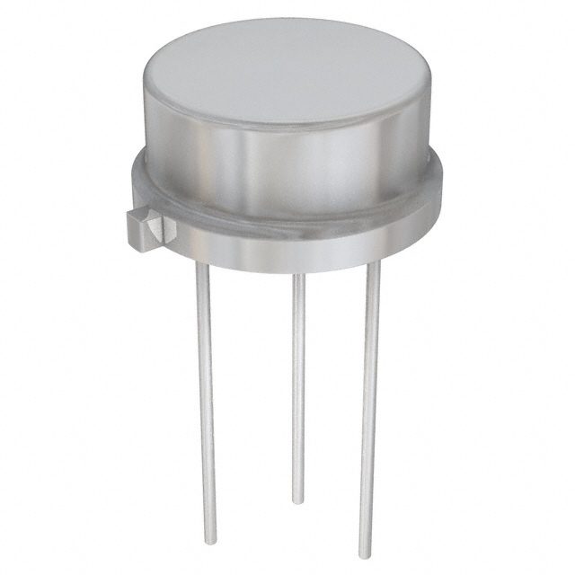
Basic Information Overview: - Category: Power MOSFET - Use: Amplification and switching in electronic circuits - Characteristics: High voltage capability, low on-resistance, fast switching speed - Package: TO-220AB - Essence: Power transistor for high-voltage applications - Packaging/Quantity: Typically packaged in reels of 1000 units
Specifications: - Drain-Source Voltage (Vdss): 200V - Continuous Drain Current (Id): 5.3A - On-Resistance (Rds(on)): 1.6Ω - Gate-Source Voltage (Vgs): ±20V - Power Dissipation (Pd): 75W
Detailed Pin Configuration: - Pin 1 (Gate): Input for controlling the transistor - Pin 2 (Drain): Output terminal for the transistor - Pin 3 (Source): Common terminal for the transistor
Functional Features: - High voltage capability allows for use in high-power applications - Low on-resistance minimizes power loss and heat generation - Fast switching speed enables efficient operation in switching circuits
Advantages: - Suitable for high-voltage applications - Low power dissipation - Fast switching speed
Disadvantages: - Relatively high on-resistance compared to some alternative models - Limited maximum gate-source voltage
Working Principles: The 2N6660JTVP02 operates based on the principles of field-effect transistors, where the flow of current between the drain and source terminals is controlled by the voltage applied to the gate terminal.
Detailed Application Field Plans: - Power supplies - Motor control - Audio amplifiers - LED lighting systems
Detailed and Complete Alternative Models: - IRF540N - FQP30N06L - STP55NF06L
This comprehensive entry provides a detailed overview of the 2N6660JTVP02 power MOSFET, including its specifications, pin configuration, functional features, advantages, disadvantages, working principles, application field plans, and alternative models.
Lista 10 Vanliga frågor och svar relaterade till tillämpningen av 2N6660JTVP02 i tekniska lösningar
What is the 2N6660JTVP02 transistor used for?
- The 2N6660JTVP02 is a high-voltage, high-speed N-channel power MOSFET designed for applications such as switching power supplies and motor control.
What are the key specifications of the 2N6660JTVP02?
- The 2N6660JTVP02 features a maximum drain-source voltage of 400V, a continuous drain current of 5A, and a low on-resistance for efficient power handling.
Can the 2N6660JTVP02 be used in high-frequency applications?
- Yes, the 2N6660JTVP02 is suitable for high-frequency switching due to its high-speed performance and low gate charge.
What are the typical applications for the 2N6660JTVP02?
- Typical applications include switch mode power supplies, DC-DC converters, motor drives, and other high-voltage, high-speed switching circuits.
Does the 2N6660JTVP02 require a heat sink for operation?
- Depending on the application and power dissipation, a heat sink may be necessary to ensure proper thermal management.
What is the maximum junction temperature of the 2N6660JTVP02?
- The 2N6660JTVP02 has a maximum junction temperature of 150°C, which should not be exceeded to maintain device reliability.
Is the 2N6660JTVP02 suitable for automotive applications?
- Yes, the 2N6660JTVP02 can be used in automotive systems such as electronic power steering, engine control, and other high-voltage automotive electronics.
What are the recommended gate drive requirements for the 2N6660JTVP02?
- The 2N6660JTVP02 requires a gate voltage sufficient to fully enhance the channel and minimize switching losses, typically around 10V.
Can the 2N6660JTVP02 be used in parallel to increase current handling capability?
- Yes, the 2N6660JTVP02 can be used in parallel to share current and improve overall power handling in high-current applications.
Are there any application notes or reference designs available for the 2N6660JTVP02?
- Yes, various application notes and reference designs are available from the manufacturer to assist in the proper implementation of the 2N6660JTVP02 in technical solutions.