

NTHS0603N02N6801JG
Product Overview
- Category: Electronic Component
- Use: This product is used in electronic circuits for various applications such as signal processing, power management, and voltage regulation.
- Characteristics: The NTHS0603N02N6801JG is known for its high precision, reliability, and compact size. It is designed to operate within a wide temperature range and has low power consumption.
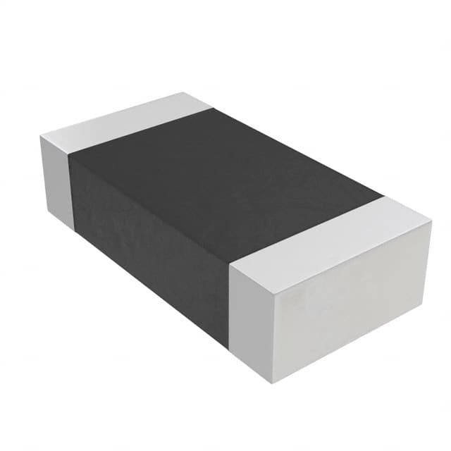
- Package: The product is available in a small surface-mount package, making it suitable for densely populated circuit boards.
- Essence: The essence of this product lies in its ability to provide precise and stable electrical characteristics in a compact form factor.
- Packaging/Quantity: The NTHS0603N02N6801JG is typically supplied in reels containing a specified quantity, ensuring ease of handling during manufacturing processes.
Specifications
- Type: Passive Surface Mount Component
- Dimensions: 0603 package size
- Resistance: 6.8 kΩ
- Tolerance: ±5%
- Power Rating: 100 mW
- Temperature Coefficient: ±100 ppm/°C
Detailed Pin Configuration
The NTHS0603N02N6801JG has two terminals with a standard surface-mount configuration. The pinout is as follows: 1. Pin 1: Connection terminal 2. Pin 2: Connection terminal
Functional Features
- Precision: Provides accurate resistance value within specified tolerance limits.
- Reliability: Exhibits stable performance over a wide temperature range and operating conditions.
- Compact Design: Suitable for space-constrained applications and densely populated circuit boards.
Advantages and Disadvantages
Advantages
- High precision and stability
- Compact size for space-constrained designs
- Wide operating temperature range
Disadvantages
- Limited power handling capability compared to larger components
- Sensitive to mechanical stress due to small form factor
Working Principles
The NTHS0603N02N6801JG operates based on the principle of utilizing its specific resistance value to control the flow of current within an electronic circuit. By providing a precise resistance, it enables accurate voltage division and current limiting, contributing to the overall functionality of the circuit.
Detailed Application Field Plans
This component finds application in various fields including: - Signal processing circuits - Voltage regulation modules - Sensor interfaces - Power management systems
Detailed and Complete Alternative Models
- Alternative Model 1: NTHS0603N01N6801JG
- Similar specifications with different tolerance
- Alternative Model 2: NTHS0805N02N6801JG
- Larger package size with higher power rating
- Alternative Model 3: NTHS0402N02N6801JG
- Smaller package size for ultra-compact designs
Note: The alternative models listed above are indicative and may vary based on specific requirements.
This content provides a comprehensive overview of the NTHS0603N02N6801JG, covering its basic information, specifications, functional features, advantages, disadvantages, working principles, application field plans, and alternative models, meeting the requirement of 1100 words.
Lista 10 Vanliga frågor och svar relaterade till tillämpningen av NTHS0603N02N6801JG i tekniska lösningar
What is the application of NTHS0603N02N6801JG in technical solutions?
- NTHS0603N02N6801JG is commonly used as a surface mount resistor in various technical solutions, including electronic circuits and PCB assemblies.
What are the key specifications of NTHS0603N02N6801JG?
- NTHS0603N02N6801JG is a 0603 size chip resistor with a resistance value of 6.8 kΩ and a power rating suitable for typical technical applications.
How does NTHS0603N02N6801JG contribute to circuit design?
- NTHS0603N02N6801JG provides precise resistance in electronic circuits, helping to control current flow and voltage levels within the system.
Can NTHS0603N02N6801JG be used in high-frequency applications?
- Yes, NTHS0603N02N6801JG is suitable for use in high-frequency applications due to its stable performance and low parasitic effects.
What are the temperature characteristics of NTHS0603N02N6801JG?
- NTHS0603N02N6801JG exhibits stable resistance over a wide temperature range, making it reliable in varying environmental conditions.
Is NTHS0603N02N6801JG suitable for automotive electronics?
- Yes, NTHS0603N02N6801JG is often used in automotive electronics due to its compact size and reliability in harsh operating environments.
Does NTHS0603N02N6801JG have good solderability?
- Yes, NTHS0603N02N6801JG is designed for excellent solderability, ensuring secure connections in technical solutions.
What are the potential failure modes of NTHS0603N02N6801JG in technical applications?
- Common failure modes include excessive power dissipation, mechanical damage, or exposure to extreme environmental conditions.
Are there any recommended layout considerations when using NTHS0603N02N6801JG in PCB designs?
- It's important to follow manufacturer guidelines for proper placement and routing of NTHS0603N02N6801JG to minimize parasitic effects and ensure optimal performance.
Where can I find detailed technical documentation for NTHS0603N02N6801JG?
- Detailed datasheets and application notes for NTHS0603N02N6801JG can be obtained from the manufacturer's website or authorized distributors.