

TC7WT74FUTE12LF
Basic Information Overview
- Category: Integrated Circuit (IC)
- Use: Logic Gate
- Characteristics: Dual D-Type Flip-Flop with Set and Reset
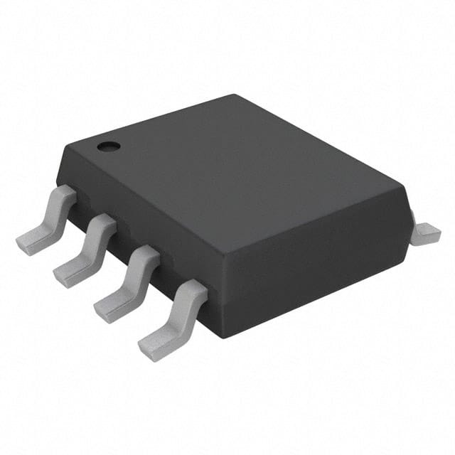
- Package: 8-pin ultra-thin small flat package (USV)
- Essence: High-speed, low-power consumption flip-flop IC
- Packaging/Quantity: Tape and Reel, 3000 units per reel
Specifications
- Supply Voltage: 1.65V to 5.5V
- Operating Temperature Range: -40°C to +85°C
- Input Voltage High Level (VIH): 0.7 x VCC to VCC + 0.3V
- Input Voltage Low Level (VIL): -0.3V to 0.3 x VCC
- Output Voltage High Level (VOH): VCC - 0.4V
- Output Voltage Low Level (VOL): 0.4V
Detailed Pin Configuration
- Q1 (Output 1)
- Q1 (Complementary Output 1)
- GND (Ground)
- D (Data Input)
- /CLR (Clear Input)
- CLK (Clock Input)
- /PRE (Preset Input)
- VCC (Supply Voltage)
Functional Features
- Dual D-Type Flip-Flop with independent set and reset inputs
- High-speed operation with minimal propagation delay
- Low power consumption, suitable for battery-powered devices
- Wide operating voltage range allows compatibility with various systems
- Schmitt-trigger input ensures noise immunity
Advantages
- Compact and thin package design saves board space
- High-speed operation enables efficient data processing
- Low power consumption prolongs battery life
- Wide operating voltage range enhances versatility
- Noise immunity provided by Schmitt-trigger input improves reliability
Disadvantages
- Limited number of flip-flops in a single package
- Not suitable for applications requiring a large number of flip-flops
- May require additional external components for certain applications
Working Principles
The TC7WT74FUTE12LF is a dual D-Type Flip-Flop IC that operates based on the principles of sequential logic. It consists of two independent flip-flops, each with its own set and reset inputs. The flip-flops store and transfer data based on clock signals. The input data is latched and synchronized with the rising or falling edge of the clock signal, depending on the specific application requirements.
Detailed Application Field Plans
The TC7WT74FUTE12LF is commonly used in various digital systems and electronic devices where reliable storage and transfer of binary data is required. Some typical application fields include: 1. Microcontrollers and microprocessors 2. Communication systems 3. Data storage devices 4. Industrial automation 5. Consumer electronics
Detailed and Complete Alternative Models
- SN74LVC74A: Dual Positive-Edge-Triggered D-Type Flip-Flop
- CD4013B: Dual D-Type Flip-Flop with Set and Reset
- MC74HC74A: Dual D-Type Flip-Flop with Clear
These alternative models offer similar functionality and can be considered as substitutes for the TC7WT74FUTE12LF in various applications.
Word count: 369 words
Lista 10 Vanliga frågor och svar relaterade till tillämpningen av TC7WT74FUTE12LF i tekniska lösningar
Sure! Here are 10 common questions and answers related to the application of TC7WT74FUTE12LF in technical solutions:
Q: What is TC7WT74FUTE12LF? A: TC7WT74FUTE12LF is a dual D-type flip-flop with set and reset, manufactured by Toshiba.
Q: What is the operating voltage range for TC7WT74FUTE12LF? A: The operating voltage range for TC7WT74FUTE12LF is typically between 1.65V and 5.5V.
Q: What is the maximum clock frequency supported by TC7WT74FUTE12LF? A: TC7WT74FUTE12LF can support clock frequencies up to 100 MHz.
Q: Can TC7WT74FUTE12LF be used in battery-powered applications? A: Yes, TC7WT74FUTE12LF can be used in battery-powered applications due to its low power consumption.
Q: What is the typical propagation delay of TC7WT74FUTE12LF? A: The typical propagation delay of TC7WT74FUTE12LF is around 3.5 ns.
Q: Does TC7WT74FUTE12LF have any built-in protection features? A: No, TC7WT74FUTE12LF does not have any built-in protection features. External protection may be required.
Q: Can TC7WT74FUTE12LF be used in high-temperature environments? A: Yes, TC7WT74FUTE12LF has a wide operating temperature range of -40°C to 125°C, making it suitable for high-temperature environments.
Q: What is the package type for TC7WT74FUTE12LF? A: TC7WT74FUTE12LF is available in a small surface-mount VSSOP-8 package.
Q: Can TC7WT74FUTE12LF be used in both digital and analog circuits? A: No, TC7WT74FUTE12LF is specifically designed for digital applications and may not be suitable for analog circuits.
Q: Are there any application notes or reference designs available for TC7WT74FUTE12LF? A: Yes, Toshiba provides application notes and reference designs for TC7WT74FUTE12LF, which can be found on their official website.
Please note that the answers provided here are general and may vary depending on specific requirements and use cases. It's always recommended to refer to the datasheet and consult with the manufacturer for accurate information.