

XC6118N09BGR-G
Product Overview
Category
XC6118N09BGR-G belongs to the category of voltage regulators.
Use
It is commonly used for regulating voltage in electronic circuits.
Characteristics
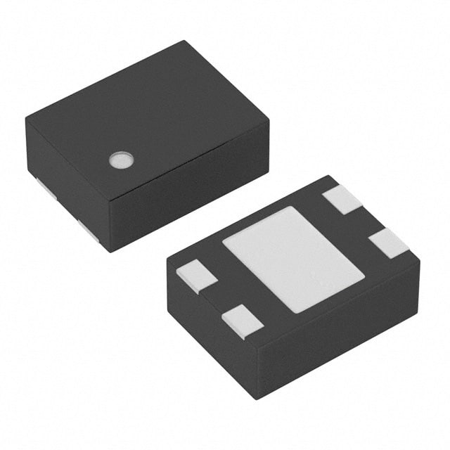
- Package: SOT-23-5
- Essence: Low dropout voltage regulator
- Packaging/Quantity: Tape and reel, 3000 units per reel
Specifications
The specifications of XC6118N09BGR-G are as follows:
- Input Voltage Range: 2.5V to 6.0V
- Output Voltage: 0.9V
- Output Current: 150mA
- Dropout Voltage: 200mV (typical)
- Quiescent Current: 30µA (typical)
- Line Regulation: ±0.1% (typical)
- Load Regulation: ±0.3% (typical)
- Operating Temperature Range: -40°C to +85°C
Detailed Pin Configuration
XC6118N09BGR-G has a total of five pins arranged as follows:
```
| | --| |-- |____| ```
Pin Configuration: 1. VIN: Input voltage pin 2. GND: Ground pin 3. EN: Enable pin 4. NC: No connection 5. VOUT: Output voltage pin
Functional Features
- Low dropout voltage: The XC6118N09BGR-G has a low dropout voltage of only 200mV, ensuring efficient regulation even when the input voltage is close to the desired output voltage.
- Low quiescent current: With a typical quiescent current of only 30µA, this voltage regulator minimizes power consumption when the load is light.
- Excellent line and load regulation: The XC6118N09BGR-G provides precise voltage regulation with ±0.1% line regulation and ±0.3% load regulation.
- Thermal shutdown protection: The device includes thermal shutdown protection to prevent damage due to excessive temperature.
Advantages and Disadvantages
Advantages: - Low dropout voltage ensures efficient regulation. - Low quiescent current minimizes power consumption. - Excellent line and load regulation for precise voltage control. - Thermal shutdown protection prevents damage from overheating.
Disadvantages: - Limited output current of 150mA may not be suitable for high-power applications. - Only available in SOT-23-5 package, limiting compatibility with certain circuit designs.
Working Principles
The XC6118N09BGR-G is a linear voltage regulator that operates by comparing the output voltage with a reference voltage. It adjusts the resistance between the input and output to maintain a constant output voltage, regardless of changes in the input voltage or load conditions. The enable pin allows the user to control the regulator's operation, providing flexibility in power management.
Detailed Application Field Plans
XC6118N09BGR-G finds applications in various electronic devices and systems, including but not limited to: - Battery-powered devices - Portable consumer electronics - IoT devices - Embedded systems - Automotive electronics - Industrial control systems
Detailed and Complete Alternative Models
Some alternative models to XC6118N09BGR-G that offer similar functionality are: - LM1117-3.3: A low dropout voltage regulator with an output voltage of 3.3V and a maximum output current of 800mA. - MCP1702-5002E/TO: A low dropout voltage regulator with an output voltage of 5.0V and a maximum output current of 250mA. - LT1763CS8-3.3: A low dropout voltage regulator with an output voltage of 3.3V and a maximum output current of 500mA.
These alternative models can be considered based on specific requirements and design constraints.
Word Count: 524 words
Lista 10 Vanliga frågor och svar relaterade till tillämpningen av XC6118N09BGR-G i tekniska lösningar
Sure! Here are 10 common questions and answers related to the application of XC6118N09BGR-G in technical solutions:
Question: What is XC6118N09BGR-G?
- Answer: XC6118N09BGR-G is a voltage detector IC (integrated circuit) that monitors the power supply voltage and provides a reset signal when the voltage drops below a certain threshold.Question: What is the operating voltage range of XC6118N09BGR-G?
- Answer: The operating voltage range of XC6118N09BGR-G is typically between 0.9V and 6.0V.Question: How does XC6118N09BGR-G help in technical solutions?
- Answer: XC6118N09BGR-G helps in technical solutions by providing a reliable reset signal to microcontrollers, DSPs, or other digital devices when the power supply voltage falls below a specified level. This ensures proper initialization and prevents data corruption.Question: What is the output type of XC6118N09BGR-G?
- Answer: XC6118N09BGR-G has an open-drain output type, which means it can be connected to other devices with a pull-up resistor to achieve the desired logic level.Question: Can XC6118N09BGR-G be used in battery-powered applications?
- Answer: Yes, XC6118N09BGR-G can be used in battery-powered applications as it has a low quiescent current consumption of typically 1.0µA, making it suitable for power-sensitive designs.Question: What is the typical reset threshold voltage of XC6118N09BGR-G?
- Answer: The typical reset threshold voltage of XC6118N09BGR-G is 0.9V, but it can be adjusted using external resistors.Question: Does XC6118N09BGR-G have a built-in delay time?
- Answer: Yes, XC6118N09BGR-G has a built-in delay time of typically 200ms to ensure stable power supply before releasing the reset signal.Question: Can XC6118N09BGR-G tolerate voltage spikes or noise on the power supply line?
- Answer: Yes, XC6118N09BGR-G has a built-in noise immunity circuit that allows it to tolerate voltage spikes or noise on the power supply line.Question: Is XC6118N09BGR-G available in different package options?
- Answer: Yes, XC6118N09BGR-G is available in various package options, including SOT-25 and USP-4B.Question: Where can I find more information about XC6118N09BGR-G?
- Answer: You can find more detailed information about XC6118N09BGR-G in the datasheet provided by the manufacturer or by contacting their technical support team.