

XC6118C39BGR-G
Product Overview
Category
XC6118C39BGR-G belongs to the category of integrated circuits (ICs).
Use
This product is commonly used in electronic devices for voltage regulation and power management.
Characteristics
- Voltage regulation capabilities
- Power management features
- Compact size
- High efficiency
- Low power consumption
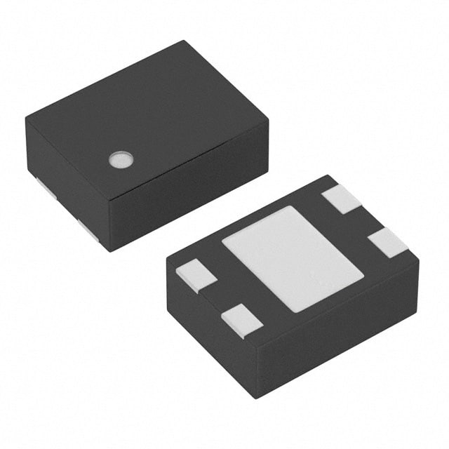
Package
XC6118C39BGR-G is available in a small form factor package, which makes it suitable for space-constrained applications.
Essence
The essence of XC6118C39BGR-G lies in its ability to regulate voltage and manage power efficiently, ensuring stable and reliable operation of electronic devices.
Packaging/Quantity
This product is typically packaged in reels or tubes, with a specific quantity per package depending on the manufacturer's specifications.
Specifications
- Input Voltage Range: 2.5V - 6.0V
- Output Voltage: 3.9V
- Output Current: Up to 100mA
- Dropout Voltage: 200mV (typical)
- Quiescent Current: 30µA (typical)
- Operating Temperature Range: -40°C to +85°C
Detailed Pin Configuration
XC6118C39BGR-G has the following pin configuration:
- VIN: Input voltage pin
- GND: Ground pin
- VOUT: Output voltage pin
- EN: Enable pin (optional)
Functional Features
- Voltage regulation: XC6118C39BGR-G ensures a stable output voltage regardless of input voltage fluctuations.
- Power management: This IC efficiently manages power consumption, reducing energy waste.
- Enable pin: The optional enable pin allows for control of the device's operation.
Advantages and Disadvantages
Advantages
- Compact size enables integration into small electronic devices.
- High efficiency results in reduced power consumption.
- Wide input voltage range allows for versatility in various applications.
Disadvantages
- Limited output current may not be suitable for high-power applications.
- Dropout voltage may cause a slight voltage drop across the device.
Working Principles
XC6118C39BGR-G utilizes internal circuitry to regulate the output voltage based on the input voltage. It employs feedback mechanisms to maintain a stable output voltage, compensating for variations in the input voltage and load conditions.
Detailed Application Field Plans
XC6118C39BGR-G finds applications in various electronic devices, including but not limited to: - Mobile phones - Portable media players - Wearable devices - IoT devices - Battery-powered devices
Detailed and Complete Alternative Models
Some alternative models that offer similar functionality to XC6118C39BGR-G are: - XC6118C39BGR - XC6118C39BGR-GP - XC6118C39BGR-GT - XC6118C39BGR-GU
These models may have slight differences in specifications or package options, but they serve the same purpose of voltage regulation and power management.
Word count: 411
Lista 10 Vanliga frågor och svar relaterade till tillämpningen av XC6118C39BGR-G i tekniska lösningar
Sure! Here are 10 common questions and answers related to the application of XC6118C39BGR-G in technical solutions:
Q: What is XC6118C39BGR-G? A: XC6118C39BGR-G is a voltage detector IC (integrated circuit) that monitors the power supply voltage and provides a reset signal when the voltage drops below a specified threshold.
Q: What is the operating voltage range of XC6118C39BGR-G? A: The operating voltage range of XC6118C39BGR-G is typically between 0.9V and 6.0V.
Q: How does XC6118C39BGR-G help in technical solutions? A: XC6118C39BGR-G helps in technical solutions by providing a reliable reset signal to microcontrollers, microprocessors, or other digital devices when the power supply voltage falls below a certain level, ensuring proper system initialization.
Q: What is the typical reset voltage threshold of XC6118C39BGR-G? A: The typical reset voltage threshold of XC6118C39BGR-G is 3.9V.
Q: Can XC6118C39BGR-G be used in battery-powered applications? A: Yes, XC6118C39BGR-G can be used in battery-powered applications as it has a low quiescent current consumption of typically 1.0µA, making it suitable for power-sensitive designs.
Q: Does XC6118C39BGR-G have any built-in delay time for the reset signal? A: Yes, XC6118C39BGR-G has a built-in delay time of typically 200ms to ensure stable power supply before releasing the reset signal.
Q: Can XC6118C39BGR-G be used in automotive applications? A: Yes, XC6118C39BGR-G is suitable for automotive applications as it meets the AEC-Q100 Grade 2 qualification standards.
Q: What is the package type of XC6118C39BGR-G? A: XC6118C39BGR-G is available in a SOT-25 package, which is a small surface-mount package with 5 pins.
Q: Is XC6118C39BGR-G compatible with both CMOS and TTL logic levels? A: Yes, XC6118C39BGR-G is compatible with both CMOS and TTL logic levels, making it versatile for various digital systems.
Q: Can XC6118C39BGR-G be used in industrial control systems? A: Yes, XC6118C39BGR-G can be used in industrial control systems as it operates reliably in a wide temperature range (-40°C to +85°C) and has excellent noise immunity.
Please note that the answers provided here are general and may vary depending on specific datasheet specifications and application requirements.