

TPS54240QDGQRQ1 - English Editing Encyclopedia Entry
Product Overview
Category
The TPS54240QDGQRQ1 belongs to the category of integrated circuits (ICs) and specifically falls under the power management ICs.
Use
This IC is primarily used for voltage regulation in various electronic devices and systems. It provides efficient power conversion and control, making it suitable for a wide range of applications.
Characteristics
- High efficiency: The TPS54240QDGQRQ1 offers high conversion efficiency, minimizing power losses during voltage regulation.
- Wide input voltage range: It can handle input voltages ranging from 4.5V to 28V, making it versatile for different power supply configurations.
- Adjustable output voltage: The output voltage can be adjusted within a specified range, allowing flexibility in meeting specific system requirements.
- Current limit protection: The IC incorporates current limit protection, safeguarding the circuitry from excessive current flow.
Package and Quantity
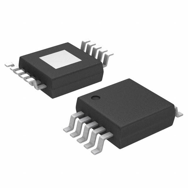
The TPS54240QDGQRQ1 is available in a small outline package (SOIC) with 10 pins. It is supplied in tape and reel packaging, with a quantity of 2500 units per reel.
Specifications
- Input Voltage Range: 4.5V to 28V
- Output Voltage Range: 0.8V to 24V
- Maximum Output Current: 2A
- Switching Frequency: 500kHz
- Operating Temperature Range: -40°C to 125°C
- Package Type: SOIC-10
Pin Configuration
The TPS54240QDGQRQ1 has the following pin configuration:
- VIN: Input voltage pin
- PGND: Power ground pin
- SW: Switching node pin
- FB: Feedback pin for output voltage regulation
- EN: Enable pin for turning the IC on/off
- SS/TR: Soft-start/Tracking pin
- COMP: Compensation pin for stability control
- VCC: Supply voltage pin
- PGND: Power ground pin
- VOUT: Output voltage pin
Functional Features
- Wide input voltage range allows compatibility with various power sources.
- Adjustable output voltage enables customization according to specific system requirements.
- High efficiency conversion minimizes power losses and improves overall energy efficiency.
- Current limit protection ensures safe operation by preventing excessive current flow.
Advantages and Disadvantages
Advantages
- High efficiency power conversion
- Wide input voltage range
- Adjustable output voltage
- Current limit protection
Disadvantages
- Limited maximum output current (2A)
Working Principles
The TPS54240QDGQRQ1 operates as a step-down (buck) converter. It uses a switching regulator topology to efficiently convert the input voltage to a lower, regulated output voltage. The IC employs pulse-width modulation (PWM) techniques to control the switching of the internal power MOSFET, achieving the desired output voltage.
Detailed Application Field Plans
The TPS54240QDGQRQ1 finds applications in various fields, including but not limited to: - Consumer electronics - Industrial automation - Telecommunications - Automotive systems - Power supplies
Detailed Alternative Models
For alternative models with similar functionality, the following options can be considered: - TPS54340QDGQRQ1 - TPS54160DGQR - LM2596S-ADJ - LT8610EMSE#PBF
These alternatives provide comparable features and can be suitable replacements depending on specific application requirements.
In conclusion, the TPS54240QDGQRQ1 is a versatile power management IC that offers high efficiency, adjustable output voltage, and current limit protection. It finds applications in various fields and has alternative models available for different design considerations.
Word Count: 470
Lista 10 Vanliga frågor och svar relaterade till tillämpningen av TPS54240QDGQRQ1 i tekniska lösningar
Sure! Here are 10 common questions and answers related to the application of TPS54240QDGQRQ1 in technical solutions:
1. What is the TPS54240QDGQRQ1? The TPS54240QDGQRQ1 is a synchronous step-down DC-DC converter with an integrated high-side MOSFET, designed for automotive applications.
2. What is the input voltage range of the TPS54240QDGQRQ1? The input voltage range of the TPS54240QDGQRQ1 is from 4.5V to 28V.
3. What is the output voltage range of the TPS54240QDGQRQ1? The output voltage range of the TPS54240QDGQRQ1 is from 0.8V to 24V.
4. What is the maximum output current of the TPS54240QDGQRQ1? The TPS54240QDGQRQ1 can deliver a maximum output current of 2A.
5. Does the TPS54240QDGQRQ1 have built-in protection features? Yes, the TPS54240QDGQRQ1 has built-in protection features such as overcurrent protection, thermal shutdown, and undervoltage lockout.
6. Can the TPS54240QDGQRQ1 operate in a wide temperature range? Yes, the TPS54240QDGQRQ1 is designed to operate in a wide temperature range from -40°C to 125°C.
7. Is the TPS54240QDGQRQ1 suitable for automotive applications? Yes, the TPS54240QDGQRQ1 is specifically designed for automotive applications and meets the AEC-Q100 Grade 1 qualification.
8. What is the efficiency of the TPS54240QDGQRQ1? The efficiency of the TPS54240QDGQRQ1 can reach up to 95% under typical operating conditions.
9. Does the TPS54240QDGQRQ1 require any external components for operation? Yes, the TPS54240QDGQRQ1 requires a few external components such as input and output capacitors, an inductor, and feedback resistors.
10. Can the TPS54240QDGQRQ1 be used in battery-powered applications? Yes, the TPS54240QDGQRQ1 is suitable for battery-powered applications due to its wide input voltage range and low quiescent current.
Please note that these questions and answers are general and may vary depending on specific application requirements.