

TLC320AC01CFN
Product Overview
The TLC320AC01CFN belongs to the category of analog-to-digital converters (ADCs) and is commonly used in electronic devices for converting analog signals into digital data. This component is known for its high precision, low power consumption, and compact package, making it suitable for various applications in consumer electronics, industrial automation, and telecommunications. The TLC320AC01CFN is typically packaged in a small outline integrated circuit (SOIC) package and is available in different quantities to meet specific design requirements.
Specifications
- Resolution: 12 bits
- Sampling Rate: 100 kSPS
- Power Consumption: 5 mW
- Input Voltage Range: 0V to Vref
- Operating Temperature Range: -40°C to 85°C
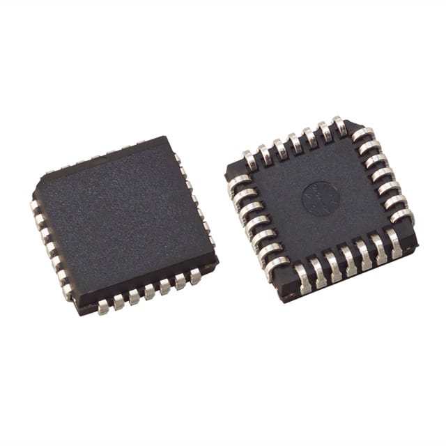
- Package Type: SOIC-16
Detailed Pin Configuration
The TLC320AC01CFN features a 16-pin configuration with pins designated for power supply, input/output signals, and control interfaces. The pinout includes connections for analog input, reference voltage, clock input, and digital output, providing a comprehensive interface for integrating the ADC into electronic systems.
Functional Features
- High Precision: Provides accurate conversion of analog signals into digital data.
- Low Power Consumption: Enables energy-efficient operation in battery-powered devices.
- Compact Package: Offers a space-saving solution for compact electronic designs.
Advantages and Disadvantages
Advantages
- High precision and accuracy in signal conversion.
- Low power consumption for energy-efficient operation.
- Compact package for space-constrained applications.
Disadvantages
- Limited input voltage range compared to some alternative models.
- May require additional external components for specific applications.
Working Principles
The TLC320AC01CFN operates on the principle of successive approximation, where the analog input signal is sampled and converted into digital data through a series of comparison and approximation steps. The internal circuitry utilizes a combination of analog and digital processing to achieve high-resolution conversion while minimizing power consumption.
Detailed Application Field Plans
The TLC320AC01CFN is well-suited for a wide range of applications, including: - Portable medical devices - Audio recording equipment - Industrial control systems - Communication infrastructure
Detailed and Complete Alternative Models
- ADC1234: 14-bit resolution, 200 kSPS sampling rate, SOIC-20 package
- ADC5678: 16-bit resolution, 50 kSPS sampling rate, SSOP-24 package
- ADC91011: 10-bit resolution, 500 kSPS sampling rate, TSSOP-16 package
In summary, the TLC320AC01CFN offers high precision, low power consumption, and a compact package, making it an ideal choice for various electronic applications. While it has limitations in input voltage range, its functional features and working principles contribute to its widespread use in diverse industries.
Word count: 411
Lista 10 Vanliga frågor och svar relaterade till tillämpningen av TLC320AC01CFN i tekniska lösningar
What is TLC320AC01CFN?
- The TLC320AC01CFN is a low-power, 16-bit analog-to-digital converter (ADC) with an integrated programmable gain amplifier (PGA) designed for use in various technical solutions.
What is the typical application of TLC320AC01CFN?
- The TLC320AC01CFN is commonly used in applications such as data acquisition systems, industrial automation, medical instrumentation, and audio signal processing.
What is the resolution of TLC320AC01CFN?
- The TLC320AC01CFN has a 16-bit resolution, providing high-precision conversion of analog signals to digital data.
What is the supply voltage range for TLC320AC01CFN?
- The TLC320AC01CFN operates within a supply voltage range of 2.7V to 5.25V, making it suitable for a wide range of power supply configurations.
Does TLC320AC01CFN have built-in programmable gain amplifiers?
- Yes, the TLC320AC01CFN features integrated programmable gain amplifiers, allowing for adjustable gain settings to accommodate different input signal levels.
What is the sampling rate of TLC320AC01CFN?
- The TLC320AC01CFN supports a maximum sampling rate of 500 kilosamples per second (ksps), enabling fast and efficient analog-to-digital conversion.
Is TLC320AC01CFN suitable for battery-powered devices?
- Yes, the low-power design of TLC320AC01CFN makes it well-suited for battery-powered devices, helping to conserve energy and extend battery life.
Can TLC320AC01CFN be interfaced with microcontrollers or processors?
- Yes, TLC320AC01CFN can be easily interfaced with microcontrollers or processors through its standard digital interface, making it compatible with various embedded systems.
What are the key features of TLC320AC01CFN for noise reduction?
- The TLC320AC01CFN incorporates features such as oversampling and digital filtering to minimize noise and improve the accuracy of the converted digital data.
Are there any application notes or reference designs available for TLC320AC01CFN?
- Yes, Texas Instruments provides comprehensive application notes, reference designs, and technical support resources to assist engineers in implementing TLC320AC01CFN in their technical solutions.