

SN74LVTH32373ZKER
Product Overview
Category
SN74LVTH32373ZKER belongs to the category of integrated circuits (ICs).
Use
This IC is commonly used for data storage and transfer applications.
Characteristics
- Low-voltage operation
- High-speed performance
- 32-bit transparent D-type latch
- 3-state outputs
- Schmitt-trigger inputs
Package
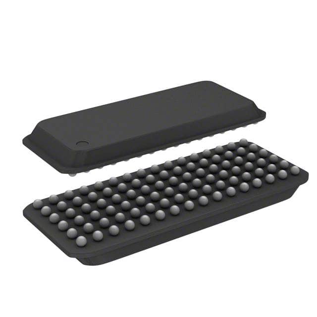
SN74LVTH32373ZKER is available in a small form factor package, such as a 56-pin BGA (Ball Grid Array) package.
Essence
The essence of SN74LVTH32373ZKER lies in its ability to store and transfer data efficiently, while operating at low voltage levels.
Packaging/Quantity
Typically, SN74LVTH32373ZKER is packaged in reels or tubes, with a quantity of 250 units per reel/tube.
Specifications
- Supply Voltage: 2.7V to 3.6V
- Input Voltage Range: 0V to VCC
- Output Voltage Range: 0V to VCC
- Operating Temperature Range: -40°C to +85°C
- Maximum Clock Frequency: 200MHz
- Output Drive Capability: ±24mA
Detailed Pin Configuration
The pin configuration of SN74LVTH32373ZKER is as follows:
- GND (Ground)
- D0 (Data Input 0)
- D1 (Data Input 1)
- D2 (Data Input 2)
- D3 (Data Input 3)
- D4 (Data Input 4)
- D5 (Data Input 5)
- D6 (Data Input 6)
- D7 (Data Input 7)
- OE (Output Enable)
- CP (Clock Pulse)
- LE (Latch Enable)
- Q0 (Output 0)
- Q1 (Output 1)
- Q2 (Output 2)
- Q3 (Output 3)
- Q4 (Output 4)
- Q5 (Output 5)
- Q6 (Output 6)
- Q7 (Output 7)
- VCC (Supply Voltage)
Functional Features
SN74LVTH32373ZKER offers the following functional features:
- Transparent latch operation
- 3-state outputs for bus sharing
- Schmitt-trigger inputs for noise immunity
- High-speed data transfer capability
- Low-voltage operation for power efficiency
Advantages and Disadvantages
Advantages
- Low-voltage operation allows for reduced power consumption.
- High-speed performance enables efficient data transfer.
- 3-state outputs facilitate bus sharing in multi-device systems.
- Schmitt-trigger inputs provide improved noise immunity.
Disadvantages
- Limited output drive capability may restrict use in certain applications requiring higher current levels.
- Availability in a specific package may limit compatibility with certain circuit designs.
Working Principles
SN74LVTH32373ZKER operates based on the principles of transparent latching. When the latch enable (LE) input is high, the data inputs (D0-D7) are transferred to the corresponding outputs (Q0-Q7). The clock pulse (CP) input controls the timing of this transfer. The output enable (OE) input determines whether the outputs are active or in a high-impedance state.
Detailed Application Field Plans
SN74LVTH32373ZKER finds application in various fields, including:
- Data storage systems
- Communication equipment
- Industrial automation
- Automotive electronics
- Consumer electronics
Detailed and Complete Alternative Models
Some alternative models that offer similar functionality to SN74LVTH32373ZKER are:
- SN74LVTH373: 8-bit transparent latch with 3-state outputs
- SN74LVTH573: 8-bit D-type flip-flop with 3-state outputs
- SN74LVTH244A: Octal buffer/line driver with 3-state outputs
These alternative models can be considered based on specific requirements and compatibility with the existing circuit design.
In conclusion, SN74LVTH32373ZKER is a versatile integrated circuit that provides efficient data storage and transfer capabilities. Its low-voltage operation, high-speed performance, and 3-state outputs make it suitable for various applications in different fields. However, its limited output drive capability and package availability should be taken into consideration when selecting this IC for a particular design.
Lista 10 Vanliga frågor och svar relaterade till tillämpningen av SN74LVTH32373ZKER i tekniska lösningar
Sure! Here are 10 common questions and answers related to the application of SN74LVTH32373ZKER:
Q: What is SN74LVTH32373ZKER? A: SN74LVTH32373ZKER is a 32-bit transparent D-type latch with 3-state outputs, designed for low-voltage (LV) operation.
Q: What is the voltage range supported by SN74LVTH32373ZKER? A: SN74LVTH32373ZKER supports a voltage range of 2.7V to 3.6V.
Q: What is the maximum data transfer rate of SN74LVTH32373ZKER? A: SN74LVTH32373ZKER has a maximum data transfer rate of 400 Mbps.
Q: Can SN74LVTH32373ZKER be used in both input and output applications? A: Yes, SN74LVTH32373ZKER can be used as both an input and output device.
Q: How many latch outputs does SN74LVTH32373ZKER have? A: SN74LVTH32373ZKER has 32 latch outputs.
Q: What is the purpose of the 3-state outputs in SN74LVTH32373ZKER? A: The 3-state outputs allow multiple devices to share a common bus without interfering with each other.
Q: Can SN74LVTH32373ZKER be cascaded to increase the number of latch outputs? A: Yes, SN74LVTH32373ZKER can be cascaded to increase the number of latch outputs in a system.
Q: Does SN74LVTH32373ZKER have any built-in protection features? A: Yes, SN74LVTH32373ZKER has built-in ESD protection to prevent damage from electrostatic discharge.
Q: What is the operating temperature range of SN74LVTH32373ZKER? A: SN74LVTH32373ZKER can operate within a temperature range of -40°C to 85°C.
Q: Are there any specific application notes or reference designs available for SN74LVTH32373ZKER? A: Yes, Texas Instruments provides application notes and reference designs that can help in implementing SN74LVTH32373ZKER in various technical solutions.
Please note that these answers are general and may vary depending on the specific requirements and use cases. It is always recommended to refer to the datasheet and documentation provided by the manufacturer for accurate information.