

SN74LVTH2952DGVR
Basic Information Overview
- Category: Integrated Circuit (IC)
- Use: Digital multiplexer/demultiplexer
- Characteristics:
- Low-voltage, high-speed CMOS technology
- Wide operating voltage range: 1.65V to 3.6V
- High-speed switching: 5.4 ns propagation delay
- Low power consumption
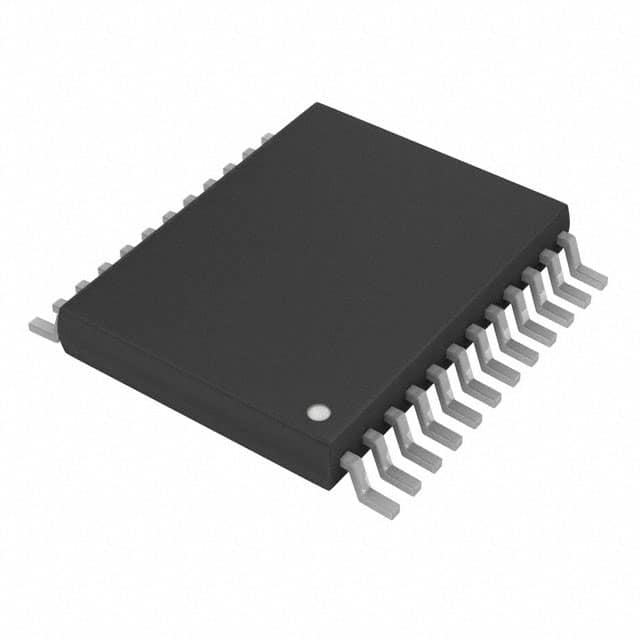
- Package: VSSOP (Very Small Outline Package)
- Essence: This IC is a multiplexer/demultiplexer that allows digital signals to be routed between multiple inputs and outputs.
- Packaging/Quantity: Available in reels of 2500 units.
Specifications
- Supply Voltage Range: 1.65V to 3.6V
- Input Voltage Range: 0V to VCC
- Output Voltage Range: 0V to VCC
- Operating Temperature Range: -40°C to +85°C
- Propagation Delay: 5.4 ns (typical)
- Input Capacitance: 3 pF (typical)
- Output Capacitance: 6 pF (typical)
- Quiescent Current: 10 μA (maximum)
Detailed Pin Configuration
The SN74LVTH2952DGVR has a total of 16 pins arranged as follows:
+-------------------+
    A0 --|1                16|-- VCC
    A1 --|2                15|-- B0
    A2 --|3                14|-- B1
    A3 --|4   SN74LVTH2952  13|-- B2
    A4 --|5     DGVR        12|-- B3
    A5 --|6                11|-- OE#
    A6 --|7                10|-- GND
    A7 --|8                 9|-- OE#
          +-------------------+
Functional Features
- Multiplexes or demultiplexes digital signals between multiple inputs and outputs.
- Wide operating voltage range allows compatibility with various systems.
- High-speed switching enables efficient data transfer.
- Low power consumption makes it suitable for battery-powered devices.
Advantages
- Versatile functionality for signal routing in digital circuits.
- Wide operating voltage range provides flexibility in system design.
- High-speed switching ensures fast data transmission.
- Low power consumption extends battery life in portable devices.
Disadvantages
- Limited number of input/output channels compared to other multiplexer/demultiplexer ICs.
- Propagation delay may affect real-time applications requiring instantaneous signal routing.
Working Principles
The SN74LVTH2952DGVR operates based on the principles of digital multiplexing and demultiplexing. It uses CMOS technology to switch digital signals between multiple inputs and outputs. The control pins (OE#) enable/disable the operation of the IC, allowing selective routing of signals. The low-voltage characteristics make it suitable for use in modern electronic systems.
Detailed Application Field Plans
The SN74LVTH2952DGVR finds applications in various fields, including: 1. Data communication systems: Used for signal routing in high-speed data transmission. 2. Telecommunications: Enables multiplexing/demultiplexing of digital signals in telecommunication networks. 3. Consumer electronics: Integrated into devices such as smartphones, tablets, and gaming consoles for signal management. 4. Industrial automation: Facilitates signal routing in control systems and industrial equipment. 5. Automotive electronics: Used in automotive systems for signal selection and routing.
Detailed and Complete Alternative Models
- CD74HC4051E: Similar multiplexer/demultiplexer IC with 8 channels.
- MC14051BCP: Analog multiplexer/demultiplexer IC with 8 channels.
- SN74HC151N: Digital multiplexer IC with 8 channels and a different pin configuration.
These alternative models offer similar functionality but may have different specifications and pin configurations. It is important to select the appropriate model based on specific requirements and system compatibility.
Word count: 459 words
Lista 10 Vanliga frågor och svar relaterade till tillämpningen av SN74LVTH2952DGVR i tekniska lösningar
Sure! Here are 10 common questions and answers related to the application of SN74LVTH2952DGVR:
Q: What is SN74LVTH2952DGVR? A: SN74LVTH2952DGVR is a multiplexer/demultiplexer IC (Integrated Circuit) that can be used for data routing and selection in various technical solutions.
Q: What is the voltage range supported by SN74LVTH2952DGVR? A: SN74LVTH2952DGVR supports a voltage range of 2.7V to 3.6V.
Q: How many channels does SN74LVTH2952DGVR have? A: SN74LVTH2952DGVR has 8 channels, allowing it to handle multiple data inputs and outputs.
Q: Can SN74LVTH2952DGVR be used as a multiplexer? A: Yes, SN74LVTH2952DGVR can be used as a multiplexer to select one of the multiple input signals and route it to a single output.
Q: Can SN74LVTH2952DGVR be used as a demultiplexer? A: Yes, SN74LVTH2952DGVR can also be used as a demultiplexer to take a single input signal and route it to one of the multiple output channels.
Q: What is the maximum data rate supported by SN74LVTH2952DGVR? A: SN74LVTH2952DGVR supports a maximum data rate of 400 Mbps (megabits per second).
Q: Does SN74LVTH2952DGVR have any built-in protection features? A: Yes, SN74LVTH2952DGVR has built-in ESD (Electrostatic Discharge) protection, which helps safeguard the IC from damage due to static electricity.
Q: Can SN74LVTH2952DGVR be used in both digital and analog applications? A: SN74LVTH2952DGVR is primarily designed for digital applications, but it can also be used in certain low-frequency analog applications.
Q: What is the power supply voltage required for SN74LVTH2952DGVR? A: SN74LVTH2952DGVR requires a power supply voltage of 3.3V.
Q: Is SN74LVTH2952DGVR available in different package options? A: Yes, SN74LVTH2952DGVR is available in various package options, including SOIC (Small Outline Integrated Circuit) and TSSOP (Thin Shrink Small Outline Package).
Please note that these answers are general and may vary depending on specific application requirements. It's always recommended to refer to the datasheet and consult with technical experts for accurate information.