

SN74LVC828ADBRG4
Product Overview
- Category: Integrated Circuit (IC)
- Use: Logic Gate
- Characteristics: Low Voltage, CMOS Technology
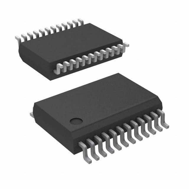
- Package: SSOP-20
- Essence: High-Speed Octal Buffer/Driver with 3-State Outputs
- Packaging/Quantity: Tape and Reel, 2500 units per reel
Specifications
- Supply Voltage Range: 1.65V to 5.5V
- High-Level Input Voltage: 2V to VCC + 0.5V
- Low-Level Input Voltage: -0.5V to 0.8V
- High-Level Output Voltage: VCC - 0.5V
- Low-Level Output Voltage: 0.5V
- Maximum Operating Frequency: 80MHz
- Propagation Delay Time: 3.9ns (Max) at 3.3V
- Output Drive Capability: ±24mA at 3.3V
Detailed Pin Configuration
The SN74LVC828ADBRG4 has a total of 20 pins arranged as follows:
___________
      |           |
   1  |         20 |  VCC
   2  |         19 |  A0
   3  |         18 |  A1
   4  |         17 |  A2
   5  |         16 |  A3
   6  |         15 |  A4
   7  |         14 |  A5
   8  |         13 |  A6
   9  |         12 |  A7
  10  |         11 |  GND
      |___________|
Functional Features
- Octal buffer/driver with 3-state outputs
- Compatible with TTL and CMOS logic levels
- High-speed operation, suitable for various applications
- Low power consumption
- Schmitt-trigger inputs for noise immunity
- ESD protection exceeds 2000V HBM per JESD22-A114 and 1000V CDM per JESD22-C101
Advantages and Disadvantages
Advantages: - Wide supply voltage range allows compatibility with different systems - High-speed operation enables efficient data transfer - Low power consumption reduces energy usage - Schmitt-trigger inputs provide noise immunity
Disadvantages: - Limited output drive capability compared to some other models - May not be suitable for applications requiring higher operating frequencies
Working Principles
The SN74LVC828ADBRG4 is an octal buffer/driver IC that amplifies and buffers digital signals. It operates using CMOS technology, which allows for low power consumption and high-speed operation. The inputs are compatible with both TTL and CMOS logic levels, making it versatile for various applications.
The device features 3-state outputs, which means they can be in one of three states: high, low, or high impedance (disconnected). This feature allows multiple devices to share a common bus without interfering with each other's signals.
The Schmitt-trigger inputs provide noise immunity by ensuring that the input signal is stable before being processed. This helps to reduce errors caused by electrical noise or signal fluctuations.
Detailed Application Field Plans
The SN74LVC828ADBRG4 is commonly used in applications where buffering and driving of digital signals are required. Some specific application fields include:
Microcontrollers and Microprocessors: The IC can be used to interface between the microcontroller/microprocessor and other peripheral devices, such as displays, memory modules, or communication interfaces.
Data Communication Systems: It can be used in data communication systems to amplify and buffer signals between different components, such as transceivers, switches, or routers.
Industrial Automation: The IC finds applications in industrial automation systems where it can be used to interface between control units, sensors, actuators, and other devices.
Automotive Electronics: It is suitable for automotive electronics applications, including vehicle control systems, infotainment systems, and communication interfaces.
Detailed and Complete Alternative Models
- SN74LVC827ADBRG4: Similar to SN74LVC828ADBRG4 but with inverted outputs.
- SN74LVC821ADBRG4: Octal buffer/driver with 2-state outputs and lower operating frequency.
- SN74LVC824ADBRG4: Octal buffer/driver with 3-state outputs and higher output drive capability.
These alternative models offer similar functionality but may have differences in terms of output configuration, operating frequency, or output drive capability. The choice of the model depends on specific application requirements.
Word count: 550 words
Lista 10 Vanliga frågor och svar relaterade till tillämpningen av SN74LVC828ADBRG4 i tekniska lösningar
Sure! Here are 10 common questions and answers related to the application of SN74LVC828ADBRG4:
1. What is the SN74LVC828ADBRG4? - The SN74LVC828ADBRG4 is a high-speed octal bus transceiver with 3-state outputs.
2. What is the operating voltage range of SN74LVC828ADBRG4? - The operating voltage range is from 1.65V to 5.5V.
3. What is the maximum data rate supported by SN74LVC828ADBRG4? - The maximum data rate is 400 Mbps.
4. How many channels does SN74LVC828ADBRG4 have? - It has 8 channels, allowing bidirectional data flow.
5. What is the purpose of the 3-state outputs in SN74LVC828ADBRG4? - The 3-state outputs allow multiple devices to share a common bus without interfering with each other.
6. Can SN74LVC828ADBRG4 be used for level shifting? - Yes, it can be used for level shifting as it supports voltage translation between different logic levels.
7. What is the typical propagation delay of SN74LVC828ADBRG4? - The typical propagation delay is around 3.9 ns.
8. Is SN74LVC828ADBRG4 compatible with both TTL and CMOS logic levels? - Yes, it is compatible with both TTL and CMOS logic levels.
9. Does SN74LVC828ADBRG4 have built-in ESD protection? - Yes, it has built-in ESD protection, making it more robust against electrostatic discharge.
10. Can SN74LVC828ADBRG4 be used in automotive applications? - Yes, it is qualified for automotive applications and meets the AEC-Q100 standard.
Please note that these answers are general and may vary depending on the specific application and requirements.