

SN74LVC2G74YEAR
Basic Information Overview
- Category: Integrated Circuit (IC)
- Use: Flip-Flop
- Characteristics: Low-voltage, dual positive-edge-triggered D-type flip-flop
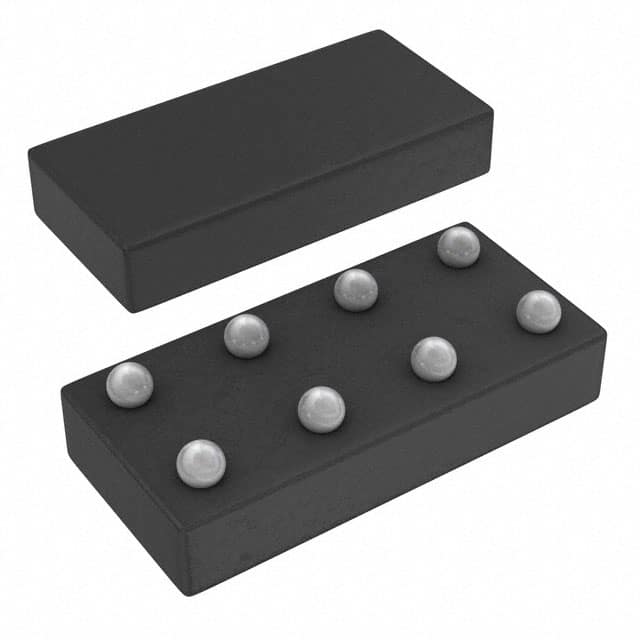
- Package: 8-pin small-outline integrated circuit (SOIC)
- Essence: Sequential logic device used for storing and transferring binary data
- Packaging/Quantity: Available in reels of 2500 units
Specifications
- Supply Voltage Range: 1.65V to 5.5V
- High-Level Input Voltage: 0.7 x VCC
- Low-Level Input Voltage: 0.3 x VCC
- High-Level Output Voltage: 0.9 x VCC
- Low-Level Output Voltage: 0.1 x VCC
- Maximum Operating Frequency: 100 MHz
- Propagation Delay Time: 4.6 ns (typical)
Detailed Pin Configuration
The SN74LVC2G74YEAR has the following pin configuration:
___________
      |           |
   1 -| CLR       |-
   2 -| D         |-
   3 -| CP        |-
   4 -| Q         |-
   5 -| GND       |-
   6 -| Q'        |-
   7 -| PRE       |-
   8 -| VCC       |-
      |___________|
Functional Features
- Dual positive-edge-triggered D-type flip-flops with clear and preset inputs
- Data is transferred to the outputs on the rising edge of the clock signal
- Clear input (CLR) sets both outputs to a low state
- Preset input (PRE) sets both outputs to a high state
- Can be used as a divide-by-two counter or frequency divider
Advantages and Disadvantages
Advantages: - Low-voltage operation allows for compatibility with a wide range of systems - Small package size enables space-saving designs - High-speed operation suitable for various applications
Disadvantages: - Limited number of flip-flops in a single package - May require additional components for complex sequential logic circuits
Working Principles
The SN74LVC2G74YEAR is a positive-edge-triggered D-type flip-flop. It stores and transfers binary data using two flip-flops. The clock input (CP) controls the transfer of data from the D input to the Q and Q' outputs. On the rising edge of the clock signal, the data at the D input is latched and appears at the outputs. The clear input (CLR) sets both outputs to a low state, while the preset input (PRE) sets both outputs to a high state.
Detailed Application Field Plans
The SN74LVC2G74YEAR can be used in various applications, including: 1. Digital communication systems 2. Microcontrollers and microprocessors 3. Data storage devices 4. Industrial automation 5. Automotive electronics
Detailed and Complete Alternative Models
Some alternative models to the SN74LVC2G74YEAR include: - CD4013B: Dual D-type flip-flop with similar characteristics - MC74HC74A: Dual positive-edge-triggered D-type flip-flop with clear and preset inputs - 74HCT74: Dual D-type flip-flop with set and reset inputs
These alternative models offer similar functionality and can be used as substitutes depending on specific requirements.
Word count: 314 words
Lista 10 Vanliga frågor och svar relaterade till tillämpningen av SN74LVC2G74YEAR i tekniska lösningar
Sure! Here are 10 common questions and answers related to the application of SN74LVC2G74YEAR in technical solutions:
Q: What is SN74LVC2G74YEAR? A: SN74LVC2G74YEAR is a dual positive-edge-triggered D-type flip-flop with clear, designed for 1.65-V to 5.5-V VCC operation.
Q: What are the key features of SN74LVC2G74YEAR? A: The key features include low power consumption, wide operating voltage range, high-speed operation, and compatibility with various logic families.
Q: What is the maximum operating frequency of SN74LVC2G74YEAR? A: The maximum operating frequency of SN74LVC2G74YEAR is typically around 100 MHz.
Q: Can SN74LVC2G74YEAR be used in battery-powered applications? A: Yes, SN74LVC2G74YEAR is suitable for battery-powered applications due to its low power consumption.
Q: How many flip-flops are there in SN74LVC2G74YEAR? A: SN74LVC2G74YEAR consists of two independent flip-flops.
Q: What is the purpose of the clear input in SN74LVC2G74YEAR? A: The clear input allows the user to reset the flip-flop to a known state.
Q: Can SN74LVC2G74YEAR operate at different supply voltages? A: Yes, SN74LVC2G74YEAR can operate within a wide supply voltage range of 1.65V to 5.5V.
Q: Is SN74LVC2G74YEAR compatible with other logic families? A: Yes, SN74LVC2G74YEAR is compatible with both TTL and CMOS logic families.
Q: What is the typical propagation delay of SN74LVC2G74YEAR? A: The typical propagation delay of SN74LVC2G74YEAR is around 3.5 ns.
Q: Can SN74LVC2G74YEAR be used in high-speed applications? A: Yes, SN74LVC2G74YEAR is designed for high-speed operation and can be used in various high-speed applications.
Please note that these answers are general and may vary depending on specific application requirements.