

SN74LVC2G66YEPR
Product Overview
- Category: Integrated Circuit (IC)
- Use: Digital Logic Gate
- Characteristics: Dual Bilateral Switch
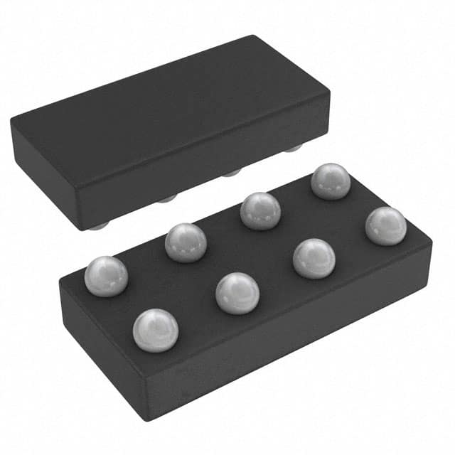
- Package: 8-pin VSSOP (Very Small Outline Package)
- Essence: High-speed CMOS technology
- Packaging/Quantity: Tape and Reel, 2500 units per reel
Specifications
- Supply Voltage Range: 1.65V to 5.5V
- Input Voltage Range: 0V to VCC
- Output Voltage Range: 0V to VCC
- Maximum Continuous Current: ±32mA
- Maximum Power Dissipation: 500mW
- Operating Temperature Range: -40°C to +85°C
Detailed Pin Configuration
The SN74LVC2G66YEPR has a total of 8 pins arranged as follows:
```
| | --| A |-- --| B |-- --| Y |-- --| GND |-- --| Y |-- --| B |-- --| A |-- |___________| ```
Pin Description: - A, B: Input pins for controlling the switch state. - Y: Output pin that connects/disconnects the two sides of the switch. - GND: Ground reference pin.
Functional Features
- Dual bilateral switch with independent control inputs.
- Low ON-state resistance and excellent ON-state current handling capability.
- Wide operating voltage range allows compatibility with various digital systems.
- Fast switching speed and low propagation delay.
- Break-before-make switching action ensures no short-circuits during transition.
Advantages and Disadvantages
Advantages: - Compact package size enables space-saving designs. - High-speed CMOS technology provides reliable performance. - Low power consumption enhances energy efficiency. - Wide supply voltage range allows compatibility with different power sources.
Disadvantages: - Limited current handling capability compared to larger switches. - Not suitable for high-power applications. - Sensitive to electrostatic discharge (ESD) and requires proper handling precautions.
Working Principles
The SN74LVC2G66YEPR is a dual bilateral switch that operates based on the control inputs provided to pins A and B. When both control inputs are low, the switch is in the OFF state, and the output pin Y is disconnected from both sides of the switch. Conversely, when either or both control inputs are high, the switch is in the ON state, and the output pin Y connects the two sides of the switch.
The switch utilizes high-speed CMOS technology, which ensures fast switching speed and low propagation delay. The break-before-make switching action prevents short-circuits during the transition between ON and OFF states.
Detailed Application Field Plans
The SN74LVC2G66YEPR finds applications in various digital systems where the need for signal routing, level shifting, or isolation arises. Some specific application areas include:
- Communication Systems: Used for signal routing and level shifting in data transmission circuits, such as UART, SPI, and I2C interfaces.
- Audio/Video Equipment: Enables audio/video signal routing and switching in devices like televisions, set-top boxes, and multimedia players.
- Industrial Control Systems: Facilitates signal routing and isolation in PLCs (Programmable Logic Controllers), motor control circuits, and sensor interfacing.
- Test and Measurement Instruments: Provides signal routing capabilities in oscilloscopes, function generators, and logic analyzers.
- Automotive Electronics: Used for signal switching and level shifting in automotive control modules, infotainment systems, and lighting controls.
Detailed and Complete Alternative Models
- CD4066BE: Quad bilateral switch with similar characteristics and pin configuration.
- TS5A23157: Dual SPDT (Single Pole Double Throw) switch with low ON-state resistance.
- MAX4617: Low-voltage, dual SPDT analog switch with high-speed performance.
These alternative models offer similar functionality and can be considered as replacements for the SN74LVC2G66YEPR in various applications.
Word count: 534 words
Lista 10 Vanliga frågor och svar relaterade till tillämpningen av SN74LVC2G66YEPR i tekniska lösningar
Sure! Here are 10 common questions and answers related to the application of SN74LVC2G66YEPR in technical solutions:
Q: What is SN74LVC2G66YEPR? A: SN74LVC2G66YEPR is a dual bilateral analog switch designed for use in various technical applications.
Q: What are the key features of SN74LVC2G66YEPR? A: Some key features include low ON-state resistance, wide operating voltage range, low power consumption, and compatibility with various logic levels.
Q: What is the purpose of using SN74LVC2G66YEPR in technical solutions? A: SN74LVC2G66YEPR is commonly used as a signal switch or multiplexer/demultiplexer in electronic circuits to control the flow of signals between different components.
Q: What is the maximum voltage rating for SN74LVC2G66YEPR? A: The maximum voltage rating for SN74LVC2G66YEPR is typically around 5.5V.
Q: Can SN74LVC2G66YEPR handle both analog and digital signals? A: Yes, SN74LVC2G66YEPR can handle both analog and digital signals, making it versatile for various applications.
Q: What is the typical ON-state resistance of SN74LVC2G66YEPR? A: The typical ON-state resistance of SN74LVC2G66YEPR is very low, usually in the range of a few ohms.
Q: Is SN74LVC2G66YEPR compatible with different logic families? A: Yes, SN74LVC2G66YEPR is compatible with a wide range of logic families, including TTL, CMOS, and LVCMOS.
Q: Can SN74LVC2G66YEPR handle high-frequency signals? A: Yes, SN74LVC2G66YEPR has a high bandwidth capability, making it suitable for handling high-frequency signals.
Q: What is the operating temperature range for SN74LVC2G66YEPR? A: The operating temperature range for SN74LVC2G66YEPR is typically between -40°C to 85°C.
Q: Are there any specific application notes or reference designs available for SN74LVC2G66YEPR? A: Yes, Texas Instruments provides application notes and reference designs that can help in implementing SN74LVC2G66YEPR in various technical solutions.
Please note that the answers provided here are general and may vary depending on the specific datasheet and manufacturer's recommendations for SN74LVC2G66YEPR.