

SN74LVC2G17YZPR
Basic Information Overview
- Category: Integrated Circuit (IC)
- Use: Logic Gate
- Characteristics: Dual Schmitt-Trigger Buffer/Driver
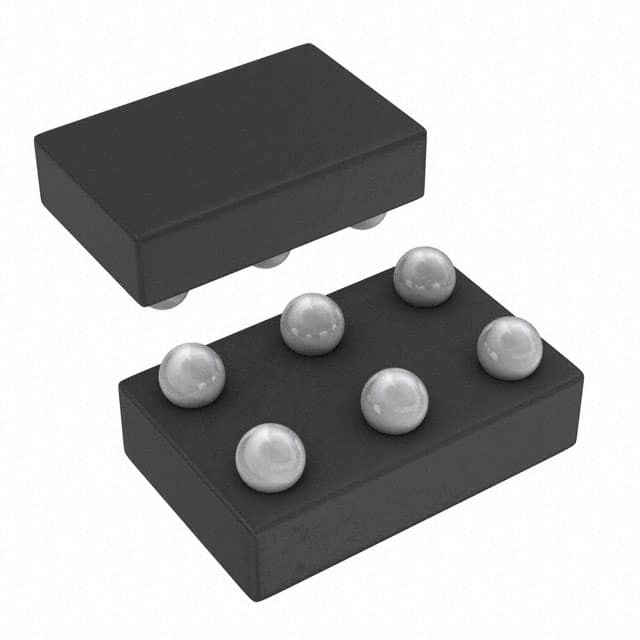
- Package: 8-pin DSBGA (MicroStar Junior™) package
- Essence: High-speed, low-power consumption buffer/driver
- Packaging/Quantity: Tape and Reel, 3000 units per reel
Specifications
- Supply Voltage Range: 1.65V to 5.5V
- Input Voltage Range: 0V to VCC
- Output Voltage Range: 0V to VCC
- High-Level Input Voltage: 0.7 x VCC to VCC
- Low-Level Input Voltage: 0V to 0.3 x VCC
- High-Level Output Voltage: 0.9 x VCC to VCC
- Low-Level Output Voltage: 0V to 0.1 x VCC
- Maximum Operating Frequency: 100 MHz
- Propagation Delay: 4.6 ns (typical)
Detailed Pin Configuration
The SN74LVC2G17YZPR has the following pin configuration:
___________
   1 -| A         |-
   2 -| Y         |-
   3 -| GND       |-
   4 -| B         |-
   5 -| Y         |-
   6 -| VCC       |-
   7 -| NC        |-
   8 -| Y         |-
       -----------
Functional Features
- Dual Schmitt-trigger buffer/driver with open-drain outputs
- Wide supply voltage range allows compatibility with various systems
- High-speed operation suitable for applications requiring fast signal propagation
- Low power consumption for energy-efficient designs
- Schmitt-trigger inputs provide hysteresis, ensuring noise immunity and signal integrity
Advantages
- Compact 8-pin package saves board space
- High-speed operation enables efficient data transmission
- Low power consumption extends battery life in portable devices
- Schmitt-trigger inputs enhance noise immunity, reducing errors in noisy environments
Disadvantages
- Limited number of input/output pins may restrict complex circuit designs
- Open-drain outputs require external pull-up resistors for proper signal levels
Working Principles
The SN74LVC2G17YZPR is a dual Schmitt-trigger buffer/driver. It accepts two input signals (A and B) and provides three output signals (Y). The Schmitt-trigger inputs ensure that the output transitions occur at different voltage levels for rising and falling input signals, providing noise immunity and preventing false triggering. The open-drain outputs require external pull-up resistors to establish the desired logic levels.
Detailed Application Field Plans
The SN74LVC2G17YZPR is commonly used in various applications, including: 1. Communication systems: Signal buffering and level shifting in UART, SPI, and I2C interfaces. 2. Industrial automation: Driving sensors, actuators, and relays in control systems. 3. Automotive electronics: Signal conditioning and interfacing in automotive modules. 4. Consumer electronics: Logic-level translation and buffering in smartphones, tablets, and gaming consoles. 5. Medical devices: Signal amplification and isolation in medical monitoring equipment.
Detailed and Complete Alternative Models
- SN74LVC2G07DCTR: Dual Buffer/Driver with Open-Drain Outputs, SOT-23 package.
- SN74LVC2G34DCUR: Dual Buffer/Driver with Schmitt-Trigger Inputs, USON-6 package.
- SN74LVC2G14DCKR: Dual Inverter with Schmitt-Trigger Inputs, SC-70 package.
- SN74LVC2G125DCUR: Dual Bus Buffer/Driver with 3-State Outputs, USON-6 package.
These alternative models offer similar functionality and can be used as substitutes for the SN74LVC2G17YZPR in various applications.
Word count: 446 words
Lista 10 Vanliga frågor och svar relaterade till tillämpningen av SN74LVC2G17YZPR i tekniska lösningar
Sure! Here are 10 common questions and answers related to the application of SN74LVC2G17YZPR:
Q: What is the SN74LVC2G17YZPR? A: The SN74LVC2G17YZPR is a dual Schmitt-trigger buffer/driver integrated circuit (IC) that can be used in various technical solutions.
Q: What is the purpose of the SN74LVC2G17YZPR? A: The SN74LVC2G17YZPR is designed to provide signal buffering and driving capabilities, particularly useful for applications involving voltage level shifting or noise immunity enhancement.
Q: What is a Schmitt-trigger? A: A Schmitt-trigger is a circuit that converts an input signal into a digital output signal with hysteresis, which helps improve noise immunity and signal integrity.
Q: What are the voltage levels supported by the SN74LVC2G17YZPR? A: The SN74LVC2G17YZPR supports voltage levels from 1.65V to 5.5V, making it compatible with a wide range of digital systems.
Q: How many channels does the SN74LVC2G17YZPR have? A: The SN74LVC2G17YZPR has two independent channels, allowing it to buffer or drive two separate signals simultaneously.
Q: Can the SN74LVC2G17YZPR be used for bidirectional communication? A: No, the SN74LVC2G17YZPR is a unidirectional buffer/driver and does not support bidirectional communication.
Q: What is the maximum output current of the SN74LVC2G17YZPR? A: The SN74LVC2G17YZPR can provide a maximum output current of 32mA, which is suitable for driving standard logic levels.
Q: Is the SN74LVC2G17YZPR capable of handling high-speed signals? A: Yes, the SN74LVC2G17YZPR has a propagation delay of only a few nanoseconds, making it suitable for high-speed applications.
Q: Can the SN74LVC2G17YZPR tolerate overvoltage or undervoltage conditions? A: The SN74LVC2G17YZPR has built-in protection features that help it tolerate overvoltage and undervoltage conditions, enhancing its robustness.
Q: What package does the SN74LVC2G17YZPR come in? A: The SN74LVC2G17YZPR is available in a small footprint, industry-standard package known as DSBGA (MicroStar Junior™), which facilitates easy integration into various designs.
Please note that these answers are general and may vary depending on specific application requirements.