

SN74LVC1G373YZPR
Product Overview
- Category: Integrated Circuit
- Use: Logic Level Shifter
- Characteristics: Single-Gate D-Type Latch with 3-State Output
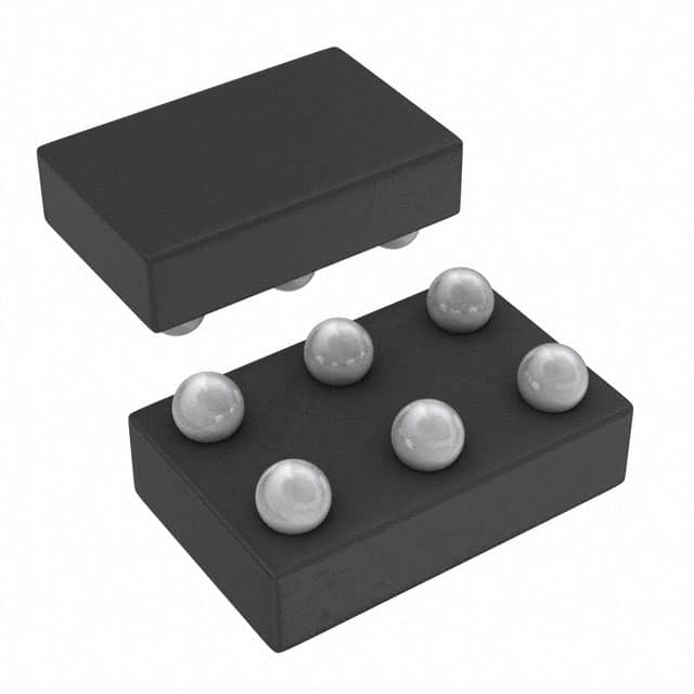
- Package: 8-Bump micro SMD package
- Essence: High-performance CMOS technology for low power consumption and high-speed operation
- Packaging/Quantity: Tape and Reel, 3000 units per reel
Specifications
The SN74LVC1G373YZPR is a single-gate D-type latch with a 3-state output. It operates on a wide voltage range from 1.65V to 5.5V, making it suitable for various applications. The latch has an active-low enable input (OE) that controls the 3-state output. It features a high-speed propagation delay of 3.8ns (typical) and a low power consumption of 2µA (maximum).
Detailed Pin Configuration
The SN74LVC1G373YZPR has the following pin configuration:
- D: Data Input
- CP: Clock Pulse Input
- OE: Output Enable Input
- Q: Latched Output
- GND: Ground
- NC: No Connection
- VCC: Power Supply
- Q̅: Complementary Output
Functional Features
- Single-gate latch with 3-state output
- High-speed operation with low propagation delay
- Wide voltage range compatibility
- Low power consumption
- Active-low output enable for control over the output state
Advantages and Disadvantages
Advantages: - High-performance CMOS technology ensures efficient operation - Wide voltage range allows for versatile use in different systems - Low power consumption minimizes energy usage - 3-state output provides flexibility in connecting multiple devices
Disadvantages: - Limited to single-gate functionality - Not suitable for applications requiring complex logic operations
Working Principles
The SN74LVC1G373YZPR operates as a latch, storing the input data (D) when the clock pulse (CP) is triggered. The latched output (Q) reflects the stored data until the output enable (OE) is activated. When OE is low, the output is enabled and reflects the stored data. Conversely, when OE is high, the output is in a high-impedance state.
Detailed Application Field Plans
The SN74LVC1G373YZPR is commonly used in various digital systems where level shifting and signal storage are required. Some specific application fields include:
- Microcontrollers: Used for interfacing with different voltage level peripherals.
- Communication Systems: Facilitates level translation between different communication protocols.
- Industrial Automation: Enables signal buffering and isolation in control systems.
- Consumer Electronics: Used in portable devices for efficient power management and signal conversion.
Detailed and Complete Alternative Models
- SN74LVC1G374DBVR: Single-Gate D-Type Latch with 3-State Output, SOT-23 package.
- SN74LVC1G373DCKR: Single-Gate D-Type Latch with 3-State Output, SC-70 package.
- SN74LVC1G373DRLR: Single-Gate D-Type Latch with 3-State Output, SOT-553 package.
These alternative models offer similar functionality and characteristics, providing options for different package preferences and system requirements.
Word count: 346 words
Lista 10 Vanliga frågor och svar relaterade till tillämpningen av SN74LVC1G373YZPR i tekniska lösningar
Sure! Here are 10 common questions and answers related to the application of SN74LVC1G373YZPR:
Q1: What is SN74LVC1G373YZPR? A1: SN74LVC1G373YZPR is a single D-type latch with 3-state output from Texas Instruments. It is commonly used in digital logic applications.
Q2: What is the voltage range supported by SN74LVC1G373YZPR? A2: SN74LVC1G373YZPR supports a voltage range of 1.65V to 5.5V, making it compatible with a wide range of systems.
Q3: How many latch outputs does SN74LVC1G373YZPR have? A3: SN74LVC1G373YZPR has one latch output, which can be either high or low based on the input conditions.
Q4: Can SN74LVC1G373YZPR be used for level shifting? A4: Yes, SN74LVC1G373YZPR can be used for level shifting as it supports both 3.3V and 5V logic levels.
Q5: What is the maximum data rate supported by SN74LVC1G373YZPR? A5: SN74LVC1G373YZPR can support data rates up to 400 Mbps, making it suitable for high-speed applications.
Q6: Does SN74LVC1G373YZPR have any built-in protection features? A6: Yes, SN74LVC1G373YZPR has built-in ESD protection, which helps safeguard against electrostatic discharge events.
Q7: Can SN74LVC1G373YZPR be used in battery-powered applications? A7: Yes, SN74LVC1G373YZPR is suitable for battery-powered applications as it has a low power consumption and wide voltage range.
Q8: What is the package type of SN74LVC1G373YZPR? A8: SN74LVC1G373YZPR comes in a small SOT-23 package, which is compact and widely used in space-constrained designs.
Q9: Can SN74LVC1G373YZPR be used in both input and output applications? A9: Yes, SN74LVC1G373YZPR can be used in both input and output applications, providing flexibility in various digital logic circuits.
Q10: Are there any application notes or reference designs available for SN74LVC1G373YZPR? A10: Yes, Texas Instruments provides application notes and reference designs for SN74LVC1G373YZPR, which can help users understand its usage in different scenarios.
Please note that these answers are general and may vary based on specific design requirements. It's always recommended to refer to the datasheet and consult with technical experts for accurate information.