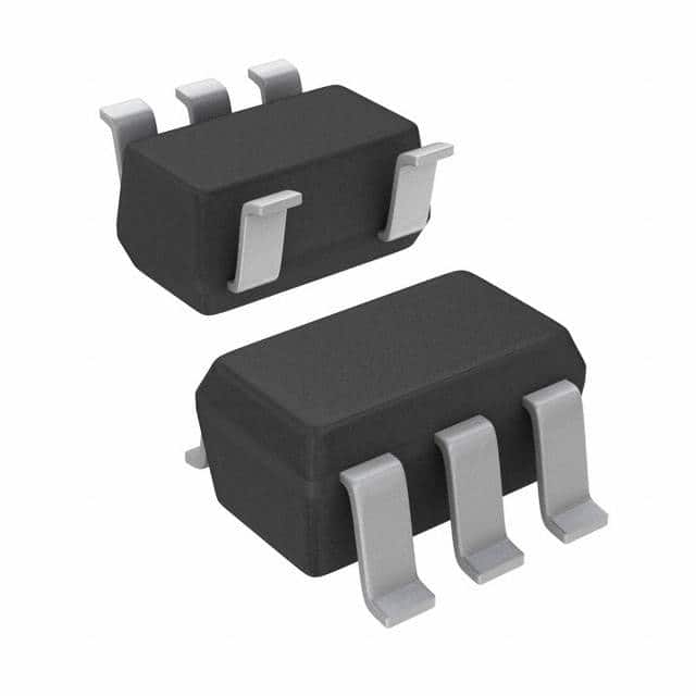
SN74LVC1G02DBVT
Product Overview
- Category: Integrated Circuit (IC)
- Use: Logic Gate
- Characteristics: Single 2-Input NOR Gate
- Package: SOT-23-5
- Essence: Digital Logic Component
- Packaging/Quantity: Tape and Reel, 3000 pieces per reel
Specifications
- Supply Voltage Range: 1.65V to 5.5V
- Input Voltage Range: -0.5V to VCC + 0.5V
- Output Voltage Range: 0V to VCC
- Maximum Operating Frequency: 100 MHz
- Propagation Delay: 3.8 ns (typical)
- Low Power Consumption: ICC = 1 µA (maximum)
Detailed Pin Configuration
The SN74LVC1G02DBVT has a total of 5 pins:
- GND (Ground): Connected to the ground reference voltage.
- A (Input A): First input terminal for the NOR gate.
- B (Input B): Second input terminal for the NOR gate.
- Y (Output): Output terminal of the NOR gate.
- VCC (Supply Voltage): Connected to the positive supply voltage.
Functional Features
- Single 2-Input NOR Gate: The SN74LVC1G02DBVT is designed to perform the logical NOR operation on two input signals.
- High-Speed Operation: With a maximum operating frequency of 100 MHz, it can process logic signals quickly.
- Wide Supply Voltage Range: It can operate within a supply voltage range of 1.65V to 5.5V, making it compatible with various systems.
- Low Power Consumption: The IC consumes very low power, with a maximum current of 1 µA.
Advantages and Disadvantages
Advantages: - Compact Size: The SOT-23-5 package allows for space-saving integration into small electronic devices. - Versatile Application: The NOR gate can be used in various digital logic circuits and systems. - Wide Supply Voltage Range: It can operate with different supply voltages, providing flexibility in system design.
Disadvantages: - Limited Functionality: The SN74LVC1G02DBVT is a single 2-input NOR gate and cannot perform other logical operations. - Propagation Delay: The propagation delay of 3.8 ns may limit its use in high-speed applications.
Working Principles
The SN74LVC1G02DBVT operates based on the principles of digital logic. It performs the NOR operation on the two input signals (A and B) and produces the logical complement of their OR function at the output (Y). The internal circuitry consists of transistors and resistors that enable the desired logic functionality.
Detailed Application Field Plans
The SN74LVC1G02DBVT finds application in various fields, including:
- Digital Electronics: It can be used in combinational logic circuits, such as adders, multiplexers, and encoders.
- Microcontrollers and Microprocessors: It serves as a building block for designing complex digital systems.
- Communication Systems: It plays a role in signal processing, data transmission, and error detection circuits.
- Industrial Automation: It contributes to control systems, PLCs (Programmable Logic Controllers), and robotics.
Detailed and Complete Alternative Models
- SN74LVC1G00DBVR: Single 2-Input NAND Gate
- SN74LVC1G04DBVR: Single Inverter (NOT Gate)
- SN74LVC1G08DBVR: Single 2-Input AND Gate
- SN74LVC1G32DBVR: Single 2-Input OR Gate
- SN74LVC1G86DBVR: Single 2-Input XOR Gate
These alternative models provide similar functionality to the SN74LVC1G02DBVT and can be used as substitutes in various applications.
Word count: 387 words
Lista 10 Vanliga frågor och svar relaterade till tillämpningen av SN74LVC1G02DBVT i tekniska lösningar
Sure! Here are 10 common questions and answers related to the application of SN74LVC1G02DBVT in technical solutions:
Q1: What is SN74LVC1G02DBVT? A1: SN74LVC1G02DBVT is a single 2-input positive-NOR gate IC (integrated circuit) that is commonly used in digital logic circuits.
Q2: What is the operating voltage range of SN74LVC1G02DBVT? A2: SN74LVC1G02DBVT operates within a voltage range of 1.65V to 5.5V.
Q3: What is the maximum output current of SN74LVC1G02DBVT? A3: The maximum output current of SN74LVC1G02DBVT is typically around 32mA.
Q4: Can SN74LVC1G02DBVT be used as a level shifter? A4: Yes, SN74LVC1G02DBVT can be used as a level shifter to convert signals between different voltage levels.
Q5: What is the typical propagation delay of SN74LVC1G02DBVT? A5: The typical propagation delay of SN74LVC1G02DBVT is around 3.6ns.
Q6: Is SN74LVC1G02DBVT suitable for high-speed applications? A6: Yes, SN74LVC1G02DBVT is designed for high-speed operation and can be used in various high-speed applications.
Q7: Can SN74LVC1G02DBVT drive capacitive loads? A7: Yes, SN74LVC1G02DBVT can drive small capacitive loads without any additional buffering.
Q8: What is the package type of SN74LVC1G02DBVT? A8: SN74LVC1G02DBVT is available in a SOT-23-5 package.
Q9: Can SN74LVC1G02DBVT be used in battery-powered applications? A9: Yes, SN74LVC1G02DBVT operates within a wide voltage range and can be used in battery-powered applications.
Q10: Are there any recommended decoupling capacitors for SN74LVC1G02DBVT? A10: It is generally recommended to use a 0.1µF ceramic capacitor placed close to the power supply pins of SN74LVC1G02DBVT for proper decoupling.
Please note that these answers are general and may vary depending on specific application requirements.


