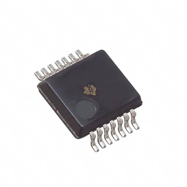
SN74LVC04ADBR
Product Overview
Category
SN74LVC04ADBR belongs to the category of integrated circuits (ICs).
Use
It is commonly used as a hex inverter, which means it performs the function of converting logic level signals from one polarity to the opposite polarity.
Characteristics
- Low voltage operation: The SN74LVC04ADBR operates at low voltage levels, typically between 1.65V and 5.5V.
- High-speed performance: It offers fast propagation delay times, making it suitable for high-speed applications.
- Wide temperature range: The IC can operate within a wide temperature range, typically between -40°C and 85°C.
- Low power consumption: It consumes minimal power, making it energy-efficient.
- Small form factor: The IC comes in a small package, allowing for space-saving designs.
Package and Quantity
The SN74LVC04ADBR is available in a surface mount package known as SSOP (Shrink Small Outline Package). It is supplied in tape and reel packaging, with a quantity of 2500 units per reel.
Specifications
- Logic Family: LVC
- Number of Inputs: 6
- Number of Outputs: 6
- Supply Voltage Range: 1.65V to 5.5V
- Propagation Delay Time: 3.8 ns (typical)
- Operating Temperature Range: -40°C to 85°C
- Package Type: SSOP
- Package Dimensions: 5.30mm x 4.40mm
Pin Configuration
The SN74LVC04ADBR has a total of 14 pins, numbered as follows:
``` __ __ |1 \/ 14| |2 13| |3 12| |4 11| |5 10| |6 9| |7 8|
```
Functional Features
- Hex Inverter: The SN74LVC04ADBR consists of six independent inverters, each capable of converting logic level signals from high to low or low to high.
- High-Speed Operation: It offers fast switching times, enabling efficient signal processing in various applications.
- Wide Voltage Range: The IC can operate at different voltage levels, providing flexibility in system design.
- Low Power Consumption: It consumes minimal power, making it suitable for battery-powered devices.
- ESD Protection: The IC incorporates electrostatic discharge (ESD) protection, enhancing its reliability and robustness.
Advantages and Disadvantages
Advantages
- Low voltage operation allows compatibility with a wide range of systems.
- High-speed performance enables efficient signal processing.
- Small form factor saves space in circuit designs.
- Low power consumption makes it suitable for portable and energy-efficient applications.
- ESD protection enhances reliability.
Disadvantages
- Limited number of inputs and outputs restricts the complexity of circuits that can be built solely using this IC.
- Lack of built-in voltage regulation may require additional components for proper voltage supply.
Working Principles
The SN74LVC04ADBR operates based on the principles of complementary metal-oxide-semiconductor (CMOS) technology. Each inverter within the IC consists of a PMOS (p-channel metal-oxide-semiconductor) transistor and an NMOS (n-channel metal-oxide-semiconductor) transistor. When the input voltage is high, the PMOS transistor turns off, while the NMOS transistor turns on, resulting in a low output voltage. Conversely, when the input voltage is low, the PMOS transistor turns on, and the NMOS transistor turns off, producing a high output voltage.
Detailed Application Field Plans
The SN74LVC04ADBR finds applications in various fields, including:
- Digital Logic Circuits: It is widely used in digital logic circuits to invert signals and perform logical operations.
- Microcontrollers and Microprocessors: The IC can be utilized in microcontroller and microprocessor-based systems for signal inversion and level shifting.
- Communication Systems: It plays a crucial role in communication systems, such as UART (Universal Asynchronous Receiver-Transmitter) interfaces, where signal polarity conversion is required.
- Consumer Electronics: The IC is commonly found in consumer electronic devices like smartphones, tablets, and gaming consoles, where it helps in signal processing and voltage level conversion.
Detailed and Complete Alternative Models
Some alternative models that offer similar functionality to the SN74LVC04ADBR include:
- 74HC04: This is a popular alternative from the 74HC series, which operates at a higher voltage range of 2V to 6V.
- CD4049: This is a hex inverter IC from the CD4000 series, which operates at a wider voltage range of 3V to
Lista 10 Vanliga frågor och svar relaterade till tillämpningen av SN74LVC04ADBR i tekniska lösningar
Sure! Here are 10 common questions and answers related to the application of SN74LVC04ADBR:
Q: What is SN74LVC04ADBR? A: SN74LVC04ADBR is a hex inverter gate IC, which means it has six independent inverters that can be used for signal inversion in digital circuits.
Q: What is the voltage range supported by SN74LVC04ADBR? A: SN74LVC04ADBR supports a voltage range from 1.65V to 5.5V, making it compatible with a wide range of digital systems.
Q: Can SN74LVC04ADBR handle high-speed signals? A: Yes, SN74LVC04ADBR is designed for high-speed operation and can handle signals with fast switching times.
Q: How much current can SN74LVC04ADBR source or sink? A: SN74LVC04ADBR can source or sink up to 32mA of current per output pin, making it suitable for driving various loads.
Q: Is SN74LVC04ADBR tolerant to overvoltage conditions? A: No, SN74LVC04ADBR is not tolerant to overvoltage conditions. It is important to ensure that the input voltage does not exceed the specified limits.
Q: Can I use SN74LVC04ADBR in battery-powered applications? A: Yes, SN74LVC04ADBR's low power consumption and wide voltage range make it suitable for battery-powered applications.
Q: Does SN74LVC04ADBR have any built-in protection features? A: SN74LVC04ADBR does not have built-in protection features. External measures should be taken to protect the IC from ESD and other potential hazards.
Q: Can I use SN74LVC04ADBR in both 3.3V and 5V systems? A: Yes, SN74LVC04ADBR is compatible with both 3.3V and 5V systems, making it versatile for various applications.
Q: What is the maximum operating temperature of SN74LVC04ADBR? A: The maximum operating temperature of SN74LVC04ADBR is typically 85°C, but it can vary depending on the specific datasheet.
Q: Are there any recommended decoupling capacitors for SN74LVC04ADBR? A: It is generally recommended to place a 0.1µF decoupling capacitor near the power supply pins of SN74LVC04ADBR to ensure stable operation.
Please note that these answers are general and may vary based on the specific requirements and datasheet of SN74LVC04ADBR.


