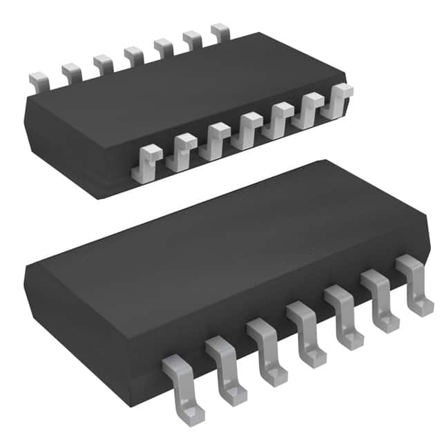
SN74LV125ATNSG4
Product Overview
- Category: Integrated Circuit (IC)
- Use: Buffer/Driver
- Characteristics: Low-voltage, Quad 3-state Non-inverting Buffer/Driver
- Package: TSSOP-14
- Essence: Logic Level Shifter
- Packaging/Quantity: Tape and Reel, 2500 units per reel
Specifications
- Supply Voltage Range: 1.65V to 5.5V
- High-level Input Voltage: 2V to VCC + 0.5V
- Low-level Input Voltage: -0.5V to 0.8V
- High-level Output Voltage: VCC - 0.5V
- Low-level Output Voltage: 0.5V
- Maximum Operating Frequency: 100MHz
- Number of Channels: 4
Detailed Pin Configuration
The SN74LV125ATNSG4 has a total of 14 pins arranged as follows:
___________
   OE | 1       14 | VCC
  A1  | 2       13 | Y1
  B1  | 3       12 | A4
  Y2  | 4       11 | B4
  A2  | 5       10 | Y4
  B2  | 6        9 | GND
  Y3  | 7        8 | A3
       ‾‾‾‾‾‾‾‾‾‾‾‾
Functional Features
- Quad non-inverting buffer/driver with 3-state outputs
- Allows voltage level shifting between different logic families
- Enables bidirectional communication between devices operating at different voltage levels
- Provides high output drive capability
- Supports both TTL and CMOS logic levels
Advantages and Disadvantages
Advantages: - Wide supply voltage range allows compatibility with various systems - 3-state outputs provide flexibility in controlling bus lines - High output drive capability ensures reliable signal transmission - Logic level shifting capability enables interfacing between different voltage domains
Disadvantages: - Limited maximum operating frequency compared to some other buffer/driver ICs - TSSOP package may require careful handling during assembly
Working Principles
The SN74LV125ATNSG4 is a non-inverting buffer/driver IC that operates as a voltage level shifter. It takes input signals from one logic family and provides output signals compatible with another logic family. The device has four independent channels, each capable of driving a single line.
The IC uses a combination of MOSFETs and CMOS technology to achieve its functionality. When the output enable (OE) pin is high, the outputs are in a high-impedance state, allowing multiple devices to share the same bus without interference. When OE is low, the inputs are buffered and transmitted to the outputs without inversion.
Detailed Application Field Plans
The SN74LV125ATNSG4 is commonly used in various applications where voltage level shifting and signal buffering are required. Some typical application fields include:
- Microcontroller Interfacing: The IC facilitates communication between microcontrollers operating at different voltage levels, enabling seamless integration of peripherals and sensors.
- Data Communication Systems: It is used in serial communication interfaces, such as UART, SPI, and I2C, to ensure proper signal translation between devices with varying voltage requirements.
- Industrial Automation: The IC finds applications in industrial control systems, PLCs, and motor drives, where it helps interface between different logic families and voltage domains.
- Automotive Electronics: It is utilized in automotive electronics for level shifting and signal buffering in various modules, such as infotainment systems, body control units, and engine management systems.
Detailed and Complete Alternative Models
- SN74LV125A: Similar to SN74LV125ATNSG4 but available in different package options (SOIC-14, PDIP-14).
- 74HC125: A compatible alternative from a different manufacturer (NXP Semiconductors) with similar functionality and pin configuration.
- CD74HCT125E: Another alternative from Texas Instruments, offering 3-state buffer/driver functionality with TTL logic compatibility.
These alternative models provide similar features and can be used as replacements for the SN74LV125ATNSG4 depending on specific requirements and availability.
Word count: 540 words
Lista 10 Vanliga frågor och svar relaterade till tillämpningen av SN74LV125ATNSG4 i tekniska lösningar
Sure! Here are 10 common questions and answers related to the application of SN74LV125ATNSG4 in technical solutions:
Q: What is SN74LV125ATNSG4? A: SN74LV125ATNSG4 is a quad bus buffer gate with 3-state outputs, commonly used for signal buffering and level shifting in digital circuits.
Q: What is the operating voltage range of SN74LV125ATNSG4? A: The operating voltage range is typically between 1.65V and 5.5V.
Q: How many channels does SN74LV125ATNSG4 have? A: SN74LV125ATNSG4 has four independent channels, each with a separate input and output.
Q: What is the maximum output current of SN74LV125ATNSG4? A: The maximum output current per channel is typically 12mA.
Q: Can SN74LV125ATNSG4 be used for level shifting between different voltage domains? A: Yes, SN74LV125ATNSG4 can be used for level shifting as long as the voltage levels are within its operating range.
Q: Does SN74LV125ATNSG4 support 3-state outputs? A: Yes, SN74LV125ATNSG4 has 3-state outputs, which means the outputs can be disabled or put into a high-impedance state.
Q: What is the propagation delay of SN74LV125ATNSG4? A: The typical propagation delay is around 5ns.
Q: Can SN74LV125ATNSG4 be used in high-speed applications? A: Yes, SN74LV125ATNSG4 is designed for high-speed operation and can be used in applications with fast switching requirements.
Q: Is SN74LV125ATNSG4 compatible with other logic families? A: Yes, SN74LV125ATNSG4 is compatible with a wide range of logic families, including TTL, CMOS, and LVTTL.
Q: What is the package type of SN74LV125ATNSG4? A: SN74LV125ATNSG4 is available in a small-outline integrated circuit (SOIC) package with 14 pins.
Please note that the answers provided here are general and may vary depending on specific datasheet specifications or application requirements.


