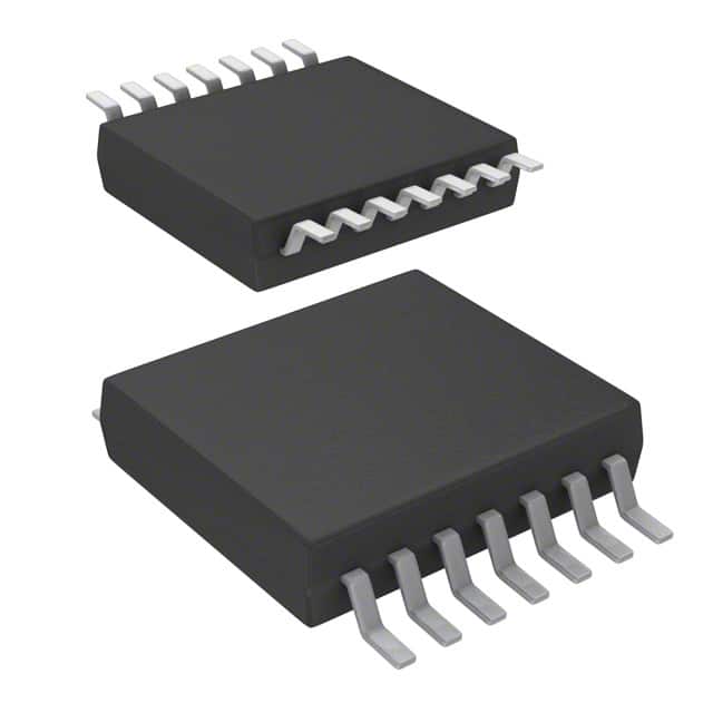
SN74LV00ADGVR
Product Overview
- Category: Integrated Circuit (IC)
- Use: Logic Gate
- Characteristics: Quad 2-Input NAND Gate
- Package: VSSOP-14
- Essence: High-performance CMOS technology
- Packaging/Quantity: Tape and Reel, 2500 pieces per reel
Specifications
- Supply Voltage Range: 1.65V to 5.5V
- Input Voltage Range: -0.5V to VCC + 0.5V
- Output Voltage Range: 0V to VCC
- Operating Temperature Range: -40°C to 85°C
- Propagation Delay Time: 4.3ns (typical)
- Maximum Quiescent Current: 10μA
Detailed Pin Configuration
The SN74LV00ADGVR has a VSSOP-14 package with the following pin configuration:
``` __ __ 1 | 1|__|14 | 4 2 | 2 13| 3 3 | 3 12| 2 4 | 4 11| 1 5 | 5 10| 6 6 | 6 9| 7 7 | 7 8| 8
Pin 1: A Input 1 Pin 2: B Input 1 Pin 3: Y Output 1 Pin 4: GND Pin 5: A Input 2 Pin 6: B Input 2 Pin 7: Y Output 2 Pin 8: VCC Pin 9: A Input 3 Pin 10: B Input 3 Pin 11: Y Output 3 Pin 12: GND Pin 13: A Input 4 Pin 14: B Input 4 ```
Functional Features
- Quad 2-input NAND gate with Schmitt-trigger inputs
- High-speed operation with low power consumption
- Wide supply voltage range allows compatibility with various systems
- Schmitt-trigger inputs provide hysteresis for improved noise immunity
- Compatible with TTL and CMOS logic levels
Advantages and Disadvantages
Advantages: - High-performance CMOS technology ensures reliable operation - Schmitt-trigger inputs enhance noise immunity - Low power consumption makes it suitable for battery-powered devices - Wide supply voltage range increases compatibility
Disadvantages: - Limited number of inputs and outputs (quad 2-input NAND gate) - Not suitable for applications requiring more complex logic functions
Working Principles
The SN74LV00ADGVR is a quad 2-input NAND gate that utilizes high-performance CMOS technology. It operates by performing the logical NAND function on two input signals, producing an inverted output. The Schmitt-trigger inputs provide hysteresis, allowing the device to tolerate noisy input signals and improve noise immunity.
Detailed Application Field Plans
The SN74LV00ADGVR can be used in various digital logic applications, including but not limited to: - Data processing systems - Communication equipment - Industrial control systems - Consumer electronics - Automotive electronics
Detailed and Complete Alternative Models
Some alternative models that offer similar functionality to the SN74LV00ADGVR include: - SN74LV00A - SN74HC00 - SN74HCT00 - CD4011B - MC14011B
These alternatives may have slight differences in specifications or package types, so it is important to refer to their respective datasheets for detailed information.
Word count: 346 words
Lista 10 Vanliga frågor och svar relaterade till tillämpningen av SN74LV00ADGVR i tekniska lösningar
Sure! Here are 10 common questions and answers related to the application of SN74LV00ADGVR:
Question: What is SN74LV00ADGVR?
- Answer: SN74LV00ADGVR is a quad 2-input NAND gate IC (integrated circuit) that is commonly used in digital logic applications.Question: What is the operating voltage range for SN74LV00ADGVR?
- Answer: The operating voltage range for SN74LV00ADGVR is typically between 1.65V and 5.5V.Question: What is the maximum output current of SN74LV00ADGVR?
- Answer: The maximum output current of SN74LV00ADGVR is typically around 8mA.Question: Can SN74LV00ADGVR be used in both CMOS and TTL logic systems?
- Answer: Yes, SN74LV00ADGVR is compatible with both CMOS and TTL logic systems.Question: What is the propagation delay of SN74LV00ADGVR?
- Answer: The propagation delay of SN74LV00ADGVR is typically around 6ns.Question: Can SN74LV00ADGVR be used in high-speed applications?
- Answer: Yes, SN74LV00ADGVR can be used in high-speed applications due to its low propagation delay.Question: Is SN74LV00ADGVR suitable for battery-powered devices?
- Answer: Yes, SN74LV00ADGVR is suitable for battery-powered devices as it operates at low voltages and has low power consumption.Question: Can SN74LV00ADGVR be used in automotive applications?
- Answer: Yes, SN74LV00ADGVR is suitable for automotive applications as it can withstand harsh environments and has a wide operating temperature range.Question: What is the package type of SN74LV00ADGVR?
- Answer: SN74LV00ADGVR comes in a small SOT-23-5 package.Question: Are there any recommended application circuits available for SN74LV00ADGVR?
- Answer: Yes, Texas Instruments provides application notes and reference designs that showcase various circuit configurations using SN74LV00ADGVR.
Please note that the answers provided here are general and may vary depending on specific datasheet specifications and application requirements.


