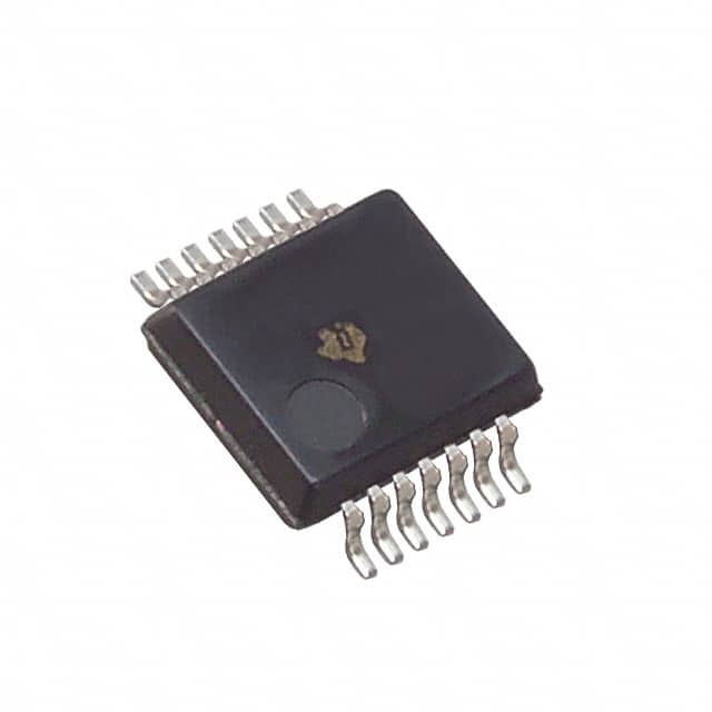
SN74LS125ADBRG4
Product Overview
- Category: Integrated Circuit
- Use: Buffer/Line Driver
- Characteristics:
- TTL Logic Level Compatibility
- High-Speed Operation
- 3-State Outputs
- Package: SOIC (Small Outline Integrated Circuit)
- Essence: Quad Bus Buffer Gates
- Packaging/Quantity: Tape and Reel, 2500 pieces per reel
Specifications
- Supply Voltage Range: 4.75V to 5.25V
- Input Voltage Range: 0V to VCC
- Output Voltage Range: 0V to VCC
- Operating Temperature Range: -40°C to +85°C
- Propagation Delay Time: 9ns (typical)
- Output Current: ±8mA
Detailed Pin Configuration
The SN74LS125ADBRG4 has a total of 14 pins arranged as follows:
__    __
   1 |1  \__/ 14| VCC
   2 |2        13| 1B
   3 |3        12| 1A
   4 |4        11| 1Y
   5 |5        10| 2Y
   6 |6         9| 2A
   7 |7         8| 2B
      |_________|
Functional Features
- Quad 3-State Non-Inverting Buffers
- Inputs and Outputs are TTL Compatible
- Enable Input for Easy Control of Output States
- High-Speed Operation for Efficient Data Transfer
Advantages and Disadvantages
Advantages: - TTL logic level compatibility ensures easy integration with existing systems. - High-speed operation allows for efficient data transfer. - 3-state outputs provide flexibility in controlling the output states.
Disadvantages: - Limited output current may not be suitable for driving certain loads. - Operating temperature range may restrict usage in extreme environments.
Working Principles
The SN74LS125ADBRG4 is a quad bus buffer gate that operates on TTL logic levels. It takes input signals and provides non-inverted, buffered outputs. The enable input allows control over the output states, making it suitable for applications where data transfer needs to be controlled. The high-speed operation ensures quick response times, while the 3-state outputs provide flexibility in managing the output states.
Detailed Application Field Plans
The SN74LS125ADBRG4 can be used in various applications, including but not limited to: - Data communication systems - Industrial automation - Automotive electronics - Consumer electronics - Medical equipment
Its compatibility with TTL logic levels and high-speed operation make it suitable for applications requiring efficient data transfer and signal buffering.
Detailed and Complete Alternative Models
Some alternative models that offer similar functionality to the SN74LS125ADBRG4 include: - SN74LS125AN - SN74LS125ADR - SN74LS125ADRG4 - SN74LS125ANE4
These models have comparable specifications and pin configurations, providing alternatives for different packaging options or availability.
Word count: 307 words
Lista 10 Vanliga frågor och svar relaterade till tillämpningen av SN74LS125ADBRG4 i tekniska lösningar
Sure! Here are 10 common questions and answers related to the application of SN74LS125ADBRG4 in technical solutions:
Q: What is SN74LS125ADBRG4? A: SN74LS125ADBRG4 is a quad bus buffer gate with 3-state outputs, commonly used in digital logic circuits.
Q: What is the operating voltage range for SN74LS125ADBRG4? A: The operating voltage range for SN74LS125ADBRG4 is typically between 4.75V and 5.25V.
Q: What is the maximum output current that SN74LS125ADBRG4 can drive? A: SN74LS125ADBRG4 can drive up to 8mA of current per output pin.
Q: Can SN74LS125ADBRG4 be used as a level shifter? A: Yes, SN74LS125ADBRG4 can be used as a level shifter to convert signals between different voltage levels.
Q: How many inputs and outputs does SN74LS125ADBRG4 have? A: SN74LS125ADBRG4 has four input pins and four output pins.
Q: What is the propagation delay of SN74LS125ADBRG4? A: The propagation delay of SN74LS125ADBRG4 is typically around 9ns.
Q: Can SN74LS125ADBRG4 be used in high-speed applications? A: While SN74LS125ADBRG4 is not specifically designed for high-speed applications, it can still be used in moderate-speed digital systems.
Q: Is SN74LS125ADBRG4 compatible with TTL logic levels? A: Yes, SN74LS125ADBRG4 is compatible with TTL logic levels and can be used in TTL-based systems.
Q: Can SN74LS125ADBRG4 be used in both input and output buffer applications? A: Yes, SN74LS125ADBRG4 can be used as both an input buffer and an output buffer in digital circuits.
Q: What is the package type for SN74LS125ADBRG4? A: SN74LS125ADBRG4 comes in a small-outline integrated circuit (SOIC) package.
Please note that these answers are general and may vary depending on specific application requirements.


