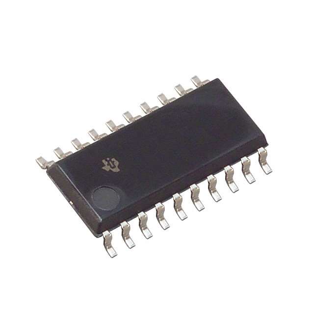
SN74HCT374ANSR
Product Overview
- Category: Integrated Circuit (IC)
- Use: Flip-Flop
- Characteristics: High-speed, CMOS technology
- Package: SOIC (Small Outline Integrated Circuit)
- Essence: 8-bit D-type flip-flop with 3-state outputs
- Packaging/Quantity: Tape and Reel, 2500 units per reel
Specifications
- Supply Voltage Range: 4.5V to 5.5V
- High-Level Input Voltage: 2V
- Low-Level Input Voltage: 0.8V
- High-Level Output Voltage: 4V
- Low-Level Output Voltage: 0.1V
- Maximum Operating Frequency: 25MHz
- Propagation Delay Time: 15ns
- Operating Temperature Range: -40°C to +85°C
Detailed Pin Configuration
The SN74HCT374ANSR has a total of 20 pins. The pin configuration is as follows:
- CLR (Clear) - Active LOW clear input
- D0 (Data Input 0) - Data input for flip-flop bit 0
- D1 (Data Input 1) - Data input for flip-flop bit 1
- D2 (Data Input 2) - Data input for flip-flop bit 2
- D3 (Data Input 3) - Data input for flip-flop bit 3
- D4 (Data Input 4) - Data input for flip-flop bit 4
- D5 (Data Input 5) - Data input for flip-flop bit 5
- D6 (Data Input 6) - Data input for flip-flop bit 6
- D7 (Data Input 7) - Data input for flip-flop bit 7
- GND (Ground) - Ground reference voltage
- Q0 (Output 0) - Output for flip-flop bit 0
- Q1 (Output 1) - Output for flip-flop bit 1
- Q2 (Output 2) - Output for flip-flop bit 2
- Q3 (Output 3) - Output for flip-flop bit 3
- Q4 (Output 4) - Output for flip-flop bit 4
- Q5 (Output 5) - Output for flip-flop bit 5
- Q6 (Output 6) - Output for flip-flop bit 6
- Q7 (Output 7) - Output for flip-flop bit 7
- OE (Output Enable) - Active LOW output enable input
- VCC (Supply Voltage) - Positive supply voltage
Functional Features
The SN74HCT374ANSR is an 8-bit D-type flip-flop with 3-state outputs. It can store and transfer data in a sequential manner. The flip-flop has a clear input (CLR) to reset all the outputs to a low state. The output enable input (OE) allows the outputs to be put into a high-impedance state, enabling multiple devices to share a common bus.
Advantages and Disadvantages
Advantages: - High-speed operation - CMOS technology provides low power consumption - 3-state outputs allow for easy bus sharing
Disadvantages: - Limited operating frequency compared to some other flip-flops - Requires external components for proper functioning
Working Principles
The SN74HCT374ANSR operates based on the principles of D-type flip-flops. It uses positive-edge triggered clocking to latch the data inputs (D0-D7) and transfer them to the outputs (Q0-Q7). The clear input (CLR) can be used to reset all the outputs to a low state. The output enable input (OE) controls whether the outputs are active or in a high-impedance state.
Detailed Application Field Plans
The SN74HCT374ANSR is commonly used in various digital systems, including:
- Microcontrollers and microprocessors
- Data storage devices
- Communication systems
- Industrial automation equipment
- Automotive electronics
Its ability to store and transfer data makes it suitable for applications that require sequential data processing and control.
Detailed and Complete Alternative Models
Some alternative models that offer similar functionality to the SN74HCT374ANSR include:
- 74HC374: This is a similar 8-bit D-type flip-flop with 3-state outputs, but it operates at a higher voltage range.
- CD74HCT374: Another 8-bit D-type flip-flop with 3-state outputs, but it uses different packaging and has slightly different specifications.
- MC74HCT374A
Lista 10 Vanliga frågor och svar relaterade till tillämpningen av SN74HCT374ANSR i tekniska lösningar
Sure! Here are 10 common questions and answers related to the application of SN74HCT374ANSR:
Q: What is SN74HCT374ANSR? A: SN74HCT374ANSR is a type of integrated circuit (IC) commonly used as an octal D-type flip-flop with 3-state outputs.
Q: What are the main features of SN74HCT374ANSR? A: The main features include 8 flip-flops with 3-state outputs, high-speed operation, compatibility with TTL inputs, and low power consumption.
Q: What is the purpose of using SN74HCT374ANSR in technical solutions? A: SN74HCT374ANSR is often used for data storage, data transfer, and signal buffering in digital systems.
Q: What is the voltage range supported by SN74HCT374ANSR? A: SN74HCT374ANSR supports a voltage range of 4.5V to 5.5V.
Q: Can SN74HCT374ANSR be used in both synchronous and asynchronous applications? A: Yes, SN74HCT374ANSR can be used in both synchronous and asynchronous applications.
Q: How many output pins does SN74HCT374ANSR have? A: SN74HCT374ANSR has 8 output pins, one for each flip-flop.
Q: What is the maximum clock frequency supported by SN74HCT374ANSR? A: The maximum clock frequency supported by SN74HCT374ANSR is typically around 25 MHz.
Q: Is SN74HCT374ANSR compatible with other logic families? A: Yes, SN74HCT374ANSR is compatible with TTL (Transistor-Transistor Logic) inputs, making it suitable for interfacing with other logic families.
Q: Can SN74HCT374ANSR be used in high-noise environments? A: Yes, SN74HCT374ANSR has built-in noise immunity features that make it suitable for use in high-noise environments.
Q: Are there any specific precautions to consider when using SN74HCT374ANSR? A: It is important to ensure proper power supply decoupling and avoid exceeding the maximum voltage and current ratings specified in the datasheet.
Please note that these answers are general and may vary depending on the specific application and requirements. Always refer to the datasheet and consult with a technical expert for accurate information.


