

SN74GTLPH16916VR
Product Overview
- Category: Integrated Circuit (IC)
- Use: Signal Level Translator
- Characteristics: High-speed, low-power, voltage level shifting
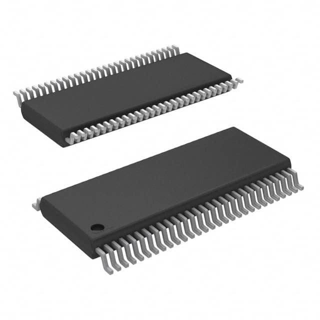
- Package: BGA (Ball Grid Array)
- Essence: Translates signals between different voltage levels
- Packaging/Quantity: Tape and Reel, 2500 units per reel
Specifications
- Supply Voltage Range: 1.2V to 3.6V
- Input Voltage Range: 0V to VCC
- Output Voltage Range: 0V to VCC
- Operating Temperature Range: -40°C to +85°C
- Number of Channels: 16
- Data Rate: Up to 2.5 Gbps
- Propagation Delay: 0.8 ns (typical)
Detailed Pin Configuration
The SN74GTLPH16916VR has a total of 56 pins. The pin configuration is as follows:
- VCCA
- VCCB
- GND
- GND
- A1
- B1
- A2
- B2
- A3
- B3
- A4
- B4
- A5
- B5
- A6
- B6
- A7
- B7
- A8
- B8
- A9
- B9
- A10
- B10
- A11
- B11
- A12
- B12
- A13
- B13
- A14
- B14
- A15
- B15
- A16
- B16
- VREF
- GND
- OE#
- GND
- VCCIOA
- VCCIOB
- A1B
- B1B
- A2B
- B2B
- A3B
- B3B
- A4B
- B4B
- A5B
- B5B
- A6B
- B6B
- A7B
- B7B
Functional Features
- Bidirectional voltage level translation between two different voltage domains
- Supports various voltage levels, making it versatile for different applications
- High-speed data transmission up to 2.5 Gbps
- Low power consumption for energy-efficient operation
- ESD (Electrostatic Discharge) protection for enhanced reliability
Advantages and Disadvantages
Advantages: - Wide supply voltage range allows compatibility with various systems - High-speed data transmission enables efficient signal processing - Low power consumption reduces energy usage - ESD protection ensures reliable operation in harsh environments
Disadvantages: - Limited number of channels (16) - Propagation delay may affect real-time applications with strict timing requirements
Working Principles
The SN74GTLPH16916VR is designed to translate signals between different voltage levels. It operates by receiving input signals from one voltage domain and converting them to the corresponding output signals in another voltage domain. This allows seamless communication between devices operating at different voltage levels.
The IC utilizes a combination of level shifters and voltage regulators to achieve accurate and reliable signal translation. The bidirectional nature of the device enables both input and output signals to be translated, ensuring compatibility between different systems.
Detailed Application Field Plans
The SN74GTLPH16916VR can be used in various applications that require voltage level translation. Some potential application fields include:
- Communication Systems: Facilitates signal translation between different voltage domains in communication systems, such as routers, switches, and network interfaces.
- Consumer Electronics: Enables compatibility between devices operating at different voltage levels, such as smartphones, tablets, and gaming consoles.
- Industrial Automation: Supports voltage level translation in industrial automation systems, including PLCs (Programmable Logic Controllers), motor control units, and sensors.
- Automotive Electronics: Provides voltage level shifting capabilities for automotive applications, such as infotainment systems, engine control units, and advanced driver-assistance systems (ADAS).
Detailed and Complete Alternative Models
- SN74LVC1T45DBVR: Single-bit dual-supply bus transceiver with voltage level translation capability.
- SN74AVC4T245PW: Quad-bit dual-supply bus transceiver with voltage level shifting functionality.
- SN74LVCH16244ADGGR: 16-bit buffer/driver with voltage level translation and direction control.
These alternative models offer similar voltage level translation features and can be considered based on specific application requirements.
*
Lista 10 Vanliga frågor och svar relaterade till tillämpningen av SN74GTLPH16916VR i tekniska lösningar
Sure! Here are 10 common questions and answers related to the application of SN74GTLPH16916VR in technical solutions:
Q: What is SN74GTLPH16916VR? A: SN74GTLPH16916VR is a high-speed differential receiver and driver IC used for signal transmission in various technical applications.
Q: What is the operating voltage range of SN74GTLPH16916VR? A: The operating voltage range of SN74GTLPH16916VR is typically between 1.2V and 3.6V.
Q: What is the maximum data rate supported by SN74GTLPH16916VR? A: SN74GTLPH16916VR supports a maximum data rate of up to 2.5 Gbps.
Q: Can SN74GTLPH16916VR be used for both single-ended and differential signaling? A: Yes, SN74GTLPH16916VR can be used for both single-ended and differential signaling applications.
Q: What is the typical input/output impedance of SN74GTLPH16916VR? A: The typical input/output impedance of SN74GTLPH16916VR is around 100 ohms.
Q: Does SN74GTLPH16916VR have built-in ESD protection? A: Yes, SN74GTLPH16916VR has built-in ESD protection to safeguard against electrostatic discharge events.
Q: Can SN74GTLPH16916VR be used in high-speed serial communication protocols like PCIe or USB? A: Yes, SN74GTLPH16916VR is suitable for use in high-speed serial communication protocols such as PCIe, USB, SATA, etc.
Q: What is the power supply current consumption of SN74GTLPH16916VR? A: The power supply current consumption of SN74GTLPH16916VR depends on the operating conditions and data rates but typically ranges from a few milliamperes to tens of milliamperes.
Q: Does SN74GTLPH16916VR support hot-plugging or hot-swapping of devices? A: Yes, SN74GTLPH16916VR supports hot-plugging and hot-swapping of devices without causing any damage to the IC.
Q: Are there any application-specific considerations when using SN74GTLPH16916VR? A: Yes, some considerations include proper termination techniques, signal integrity analysis, and adhering to the recommended layout guidelines provided in the datasheet.
Please note that these answers are general and may vary depending on the specific implementation and requirements of your technical solution.