

SN74AUP1G74RSER
Product Overview
- Category: Integrated Circuit (IC)
- Use: Flip-Flop
- Characteristics: Single D-Type Positive-Edge-Triggered Flip-Flop
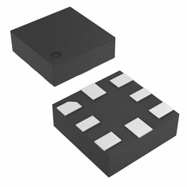
- Package: Small Outline Package (SOT-23)
- Essence: High-speed, low-power consumption flip-flop
- Packaging/Quantity: Tape and Reel, 3000 units per reel
Specifications
- Supply Voltage Range: 0.8V to 3.6V
- High-Speed Operation: 5.4 ns maximum propagation delay time
- Low Power Consumption: 0.9 µA typical ICC
- Operating Temperature Range: -40°C to +125°C
- Input/Output Compatibility: CMOS/TTL
Detailed Pin Configuration
The SN74AUP1G74RSER has a total of 5 pins:
- GND (Ground): Connected to the ground reference of the circuit.
- Q (Output): Output pin for the flip-flop.
- D (Data): Input pin for the flip-flop.
- CLK (Clock): Clock input pin for triggering the flip-flop.
- VCC (Power): Connected to the positive power supply voltage.
Functional Features
- Single D-Type Positive-Edge-Triggered Flip-Flop: The flip-flop stores and outputs a single data bit based on the rising edge of the clock signal.
- High-Speed Operation: Provides fast response times, making it suitable for applications requiring quick data storage and retrieval.
- Low Power Consumption: Consumes minimal power, making it ideal for battery-powered devices or energy-efficient designs.
- Wide Supply Voltage Range: Operates reliably within a broad range of supply voltages, enhancing versatility in various applications.
- Input/Output Compatibility: Compatible with both CMOS and TTL logic levels, allowing seamless integration with different circuitry.
Advantages and Disadvantages
Advantages: - High-speed operation enables efficient data processing. - Low power consumption prolongs battery life in portable devices. - Wide supply voltage range offers flexibility in power supply design. - Compatibility with CMOS and TTL logic levels simplifies circuit integration.
Disadvantages: - Limited functionality as a single flip-flop, may require additional components for more complex operations. - Small package size may pose challenges during manual soldering or handling.
Working Principles
The SN74AUP1G74RSER is a positive-edge-triggered flip-flop. It stores and outputs a single data bit based on the rising edge of the clock signal. When the clock input (CLK) transitions from low to high, the data input (D) is sampled and stored in the flip-flop. The stored value is then available at the output (Q). The flip-flop remains in this state until the next rising edge of the clock signal, where it captures and updates the input data.
Detailed Application Field Plans
The SN74AUP1G74RSER can be used in various applications, including but not limited to:
- Digital Communication Systems: Used for data synchronization and buffering in communication protocols such as UART, SPI, and I2C.
- Microcontrollers and Processors: Employed for register storage and control signal generation in embedded systems.
- Memory Modules: Utilized for address decoding and data storage in memory circuits.
- Sensor Interfaces: Integrated into sensor circuits for signal conditioning and timing control.
- Consumer Electronics: Incorporated in portable devices, smart appliances, and wearable technology for data processing and control functions.
Detailed and Complete Alternative Models
- SN74AUP1G74DCKR: Similar specifications and pin configuration, offered in SC-70 package.
- SN74LVC1G74DBVR: Alternative flip-flop with different characteristics, offered in SOT-23 package.
- SN74HC74N: D-Type Flip-Flop with complementary outputs, available in DIP-14 package.
These alternative models provide similar functionality and can be considered based on specific design requirements.
Word count: 496 words
Lista 10 Vanliga frågor och svar relaterade till tillämpningen av SN74AUP1G74RSER i tekniska lösningar
Sure! Here are 10 common questions and answers related to the application of SN74AUP1G74RSER in technical solutions:
Q1: What is the SN74AUP1G74RSER? A1: The SN74AUP1G74RSER is a single positive-edge-triggered D-type flip-flop with clear and preset, designed for 1.65-V to 3.6-V VCC operation.
Q2: What are the key features of SN74AUP1G74RSER? A2: The key features include low power consumption, wide operating voltage range, high-speed operation, and compatibility with various logic families.
Q3: What is the typical application of SN74AUP1G74RSER? A3: The SN74AUP1G74RSER can be used in applications such as data storage, synchronization, frequency division, and general-purpose flip-flop circuits.
Q4: What is the operating voltage range of SN74AUP1G74RSER? A4: The operating voltage range is from 1.65V to 3.6V.
Q5: What is the maximum clock frequency supported by SN74AUP1G74RSER? A5: The maximum clock frequency supported is typically around 200 MHz.
Q6: Can SN74AUP1G74RSER be used in battery-powered devices? A6: Yes, SN74AUP1G74RSER is suitable for battery-powered devices due to its low power consumption.
Q7: Is SN74AUP1G74RSER compatible with other logic families? A7: Yes, SN74AUP1G74RSER is compatible with various logic families such as CMOS, TTL, and LVCMOS.
Q8: Does SN74AUP1G74RSER have any built-in protection features? A8: Yes, SN74AUP1G74RSER has built-in ESD (electrostatic discharge) protection to prevent damage from static electricity.
Q9: Can SN74AUP1G74RSER be used in high-speed applications? A9: Yes, SN74AUP1G74RSER is designed for high-speed operation and can be used in applications that require fast switching times.
Q10: Are there any recommended external components to use with SN74AUP1G74RSER? A10: It is recommended to use decoupling capacitors near the power supply pins to ensure stable operation and minimize noise.