

SN74AUP1G57YZPR
Product Overview
- Category: Integrated Circuit
- Use: Logic Gate
- Characteristics: Single 2-Input Multiplexer
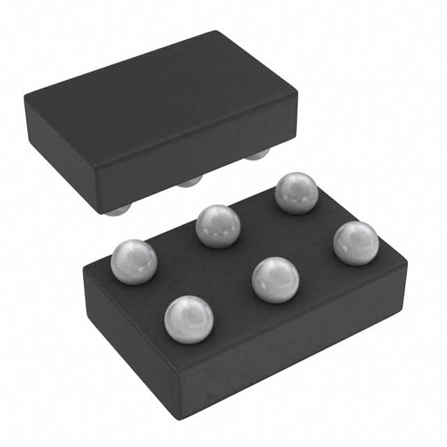
- Package: DSBGA (Y)
- Essence: High-Speed CMOS Technology
- Packaging/Quantity: Tape and Reel, 3000 pieces per reel
Specifications
The SN74AUP1G57YZPR is a single 2-input multiplexer integrated circuit. It is designed using high-speed CMOS technology, making it suitable for various digital logic applications. The device comes in a small DSBGA package (Y) and is supplied in tape and reel packaging with 3000 pieces per reel.
Detailed Pin Configuration
The SN74AUP1G57YZPR has the following pin configuration:
- Pin 1: Select Input (S)
- Pin 2: Data Input 0 (D0)
- Pin 3: Data Input 1 (D1)
- Pin 4: Output (Y)
- Pin 5: Ground (GND)
- Pin 6: Power Supply (VCC)
Functional Features
The main function of the SN74AUP1G57YZPR is to select one of the two input signals (D0 or D1) based on the select input (S). The selected input is then routed to the output pin (Y). This allows for data routing and selection in digital systems.
Advantages and Disadvantages
Advantages: - High-speed operation due to CMOS technology - Small package size for space-constrained applications - Low power consumption - Wide operating voltage range
Disadvantages: - Limited number of inputs and outputs - Not suitable for complex logic functions
Working Principles
The SN74AUP1G57YZPR operates based on the principles of digital logic. The select input (S) determines which data input (D0 or D1) is connected to the output pin (Y). When S is low, D0 is selected, and when S is high, D1 is selected. The device uses CMOS technology, which allows for fast switching and low power consumption.
Detailed Application Field Plans
The SN74AUP1G57YZPR can be used in various applications, including but not limited to: - Data routing and selection in microcontrollers - Signal multiplexing in communication systems - Address decoding in memory circuits - Input selection in digital audio/video equipment
Detailed and Complete Alternative Models
Some alternative models that offer similar functionality to the SN74AUP1G57YZPR include: - CD4053B: Triple 2-Channel Analog Multiplexer/Demultiplexer - 74HC157: Quad 2-Input Multiplexer - SN74LVC1G53: Single 2-Input Multiplexer with Schmitt-Trigger Inputs
These alternative models provide different package options, voltage ranges, and additional features, allowing users to choose the most suitable option for their specific application requirements.
Word count: 297 words
Lista 10 Vanliga frågor och svar relaterade till tillämpningen av SN74AUP1G57YZPR i tekniska lösningar
Sure! Here are 10 common questions and answers related to the application of SN74AUP1G57YZPR in technical solutions:
Q1: What is SN74AUP1G57YZPR? A1: SN74AUP1G57YZPR is a single configurable multiple-function gate that can be used in various technical applications.
Q2: What is the operating voltage range for SN74AUP1G57YZPR? A2: The operating voltage range for SN74AUP1G57YZPR is typically between 0.8V and 3.6V.
Q3: What are the different functions that SN74AUP1G57YZPR can perform? A3: SN74AUP1G57YZPR can function as a buffer, AND gate, OR gate, NAND gate, NOR gate, XOR gate, XNOR gate, or as a multiplexer.
Q4: What is the maximum output current of SN74AUP1G57YZPR? A4: The maximum output current of SN74AUP1G57YZPR is typically around 32mA.
Q5: Can SN74AUP1G57YZPR be used in high-speed applications? A5: Yes, SN74AUP1G57YZPR is designed for high-speed operation and can be used in such applications.
Q6: What is the package type for SN74AUP1G57YZPR? A6: SN74AUP1G57YZPR comes in a small SOT-23 package.
Q7: Is SN74AUP1G57YZPR compatible with other logic families? A7: Yes, SN74AUP1G57YZPR is compatible with both CMOS and TTL logic families.
Q8: Can SN74AUP1G57YZPR be used in battery-powered applications? A8: Yes, SN74AUP1G57YZPR has a low power consumption and can be used in battery-powered applications.
Q9: What is the typical propagation delay of SN74AUP1G57YZPR? A9: The typical propagation delay of SN74AUP1G57YZPR is around 2.5ns.
Q10: Can SN74AUP1G57YZPR be used in automotive applications? A10: Yes, SN74AUP1G57YZPR is AEC-Q100 qualified and can be used in automotive applications.
Please note that these answers are general and may vary depending on specific datasheet specifications and application requirements.