

SN74AUC125RGYR
Product Overview
- Category: Integrated Circuit (IC)
- Use: Buffer/Driver
- Characteristics: High-speed, low-power, non-inverting
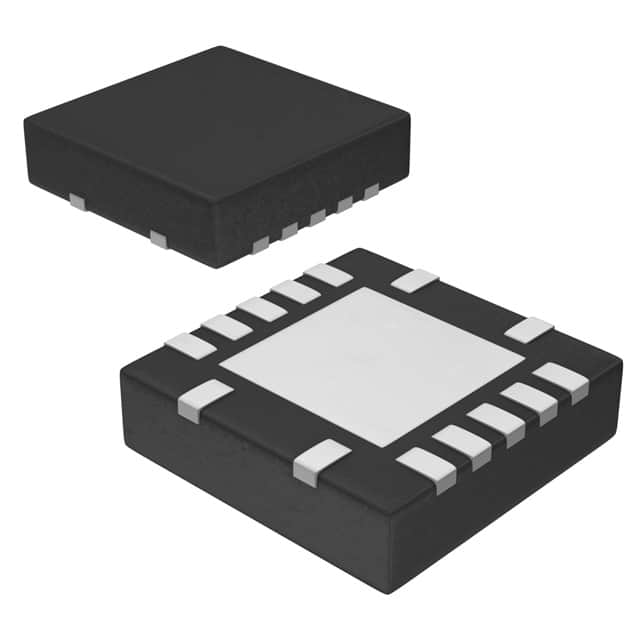
- Package: 14-pin VQFN (Very Thin Quad Flat No-Lead)
- Essence: Logic level translator
- Packaging/Quantity: Tape and reel, 2500 units per reel
Specifications
- Supply Voltage Range: 1.65V to 3.6V
- Input Voltage Range: 0V to VCC
- Output Voltage Range: 0V to VCC
- Maximum Operating Frequency: 500MHz
- Number of Channels: 4
- Input/Output Type: Non-Inverting
- Propagation Delay: 2.5ns (typical)
- Output Drive Capability: ±24mA
Detailed Pin Configuration
The SN74AUC125RGYR has a total of 14 pins, numbered as follows:
- GND (Ground)
- A1 (Input A1)
- Y1 (Output Y1)
- A2 (Input A2)
- Y2 (Output Y2)
- GND (Ground)
- A3 (Input A3)
- Y3 (Output Y3)
- A4 (Input A4)
- Y4 (Output Y4)
- VCC (Supply Voltage)
- OE (Output Enable)
- GND (Ground)
- GND (Ground)
Functional Features
- High-speed logic level translation between different voltage domains
- Non-inverting buffer/driver functionality
- Low power consumption
- Wide supply voltage range for compatibility with various systems
- Output enable pin for easy control of output state
Advantages and Disadvantages
Advantages: - High-speed operation allows for efficient data transmission - Low power consumption helps in reducing overall system energy requirements - Non-inverting functionality simplifies signal processing - Wide supply voltage range enables compatibility with different systems
Disadvantages: - Limited number of channels (4) - Propagation delay may affect timing-sensitive applications
Working Principles
The SN74AUC125RGYR is a buffer/driver IC that performs logic level translation between different voltage domains. It takes input signals from one voltage domain and provides corresponding output signals in another voltage domain. The non-inverting nature of the device ensures that the output signal matches the input signal polarity.
The IC operates by receiving input signals on the A1, A2, A3, and A4 pins. These signals are then processed internally and provided as outputs on the Y1, Y2, Y3, and Y4 pins. The OE (Output Enable) pin controls the state of the output signals, allowing them to be enabled or disabled as required.
Detailed Application Field Plans
The SN74AUC125RGYR can be used in various applications where logic level translation and buffering are required. Some potential application fields include:
- Microcontrollers: The IC can be used to interface microcontrollers operating at different voltage levels.
- Communication Systems: It can be employed in communication systems to translate logic levels between different components.
- Industrial Automation: The IC finds utility in industrial automation systems where multiple voltage domains need to be interconnected.
- Consumer Electronics: It can be utilized in consumer electronic devices to enable communication between different subsystems.
Detailed and Complete Alternative Models
- SN74AUC125RGYR - 14-pin VQFN package, 4-channel buffer/driver
- SN74LVC125ARGYR - 14-pin VQFN package, 4-channel non-inverting buffer/driver
- SN74HC125N - 14-pin DIP package, 4-channel non-inverting buffer/driver
- SN74LV1T34DBVR - SOT-23 package, single-channel non-inverting buffer
These alternative models offer similar functionality and can be considered as substitutes for the SN74AUC125RGYR depending on specific requirements.
Word count: 511 words
Lista 10 Vanliga frågor och svar relaterade till tillämpningen av SN74AUC125RGYR i tekniska lösningar
Sure! Here are 10 common questions and answers related to the application of SN74AUC125RGYR in technical solutions:
Q: What is SN74AUC125RGYR? A: SN74AUC125RGYR is a quad buffer/line driver with 3-state outputs, designed for use in various digital logic applications.
Q: What is the operating voltage range of SN74AUC125RGYR? A: The operating voltage range of SN74AUC125RGYR is typically between 0.8V and 3.6V.
Q: What is the maximum output current that SN74AUC125RGYR can drive? A: SN74AUC125RGYR can drive up to 24mA of output current per channel.
Q: Can SN74AUC125RGYR be used in both 5V and 3.3V systems? A: Yes, SN74AUC125RGYR is compatible with both 5V and 3.3V systems, making it versatile for different applications.
Q: What is the propagation delay of SN74AUC125RGYR? A: The typical propagation delay of SN74AUC125RGYR is around 2.9ns.
Q: Is SN74AUC125RGYR suitable for high-speed data transmission? A: Yes, SN74AUC125RGYR is designed for high-speed operation and can be used in applications requiring fast data transmission.
Q: Does SN74AUC125RGYR have built-in ESD protection? A: Yes, SN74AUC125RGYR has built-in ESD protection, which helps safeguard the device against electrostatic discharge.
Q: Can SN74AUC125RGYR be used in automotive applications? A: Yes, SN74AUC125RGYR is qualified for automotive applications and meets the necessary standards for automotive use.
Q: How many channels does SN74AUC125RGYR have? A: SN74AUC125RGYR has four independent buffer/line driver channels.
Q: What is the package type of SN74AUC125RGYR? A: SN74AUC125RGYR is available in a small-outline integrated circuit (SOIC) package with 14 pins.
Please note that these answers are general and may vary depending on specific datasheet information or application requirements.