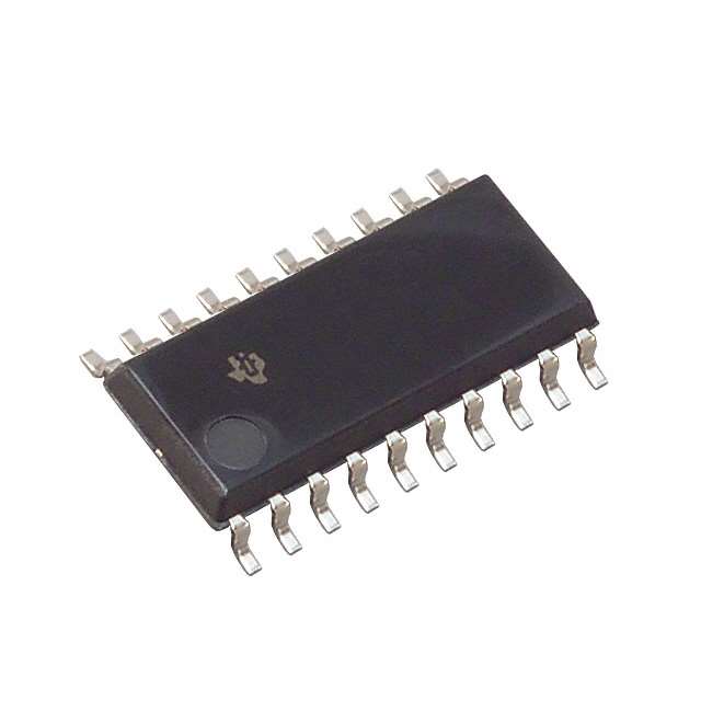
SN74AS374NSR
Product Overview
- Category: Integrated Circuit (IC)
- Use: Flip-Flop
- Characteristics: High-speed, low-power consumption
- Package: 20-pin plastic small outline package (SO)
- Essence: D-type positive-edge-triggered flip-flop
- Packaging/Quantity: Tape and reel, 2500 units per reel
Specifications
- Logic Family: AS
- Logic Type: D-Type Flip-Flop
- Number of Elements: 8
- Number of Bits per Element: 1
- Clock Edge: Positive
- Propagation Delay Time: 9 ns (typical)
- Operating Voltage Range: 4.5V to 5.5V
- Operating Temperature Range: -40°C to +85°C
Detailed Pin Configuration
The SN74AS374NSR has a total of 20 pins. The pin configuration is as follows:
- CLR (Clear)
- D0 (Data Input 0)
- D1 (Data Input 1)
- D2 (Data Input 2)
- D3 (Data Input 3)
- D4 (Data Input 4)
- D5 (Data Input 5)
- D6 (Data Input 6)
- D7 (Data Input 7)
- GND (Ground)
- Q0 (Flip-Flop Output 0)
- Q1 (Flip-Flop Output 1)
- Q2 (Flip-Flop Output 2)
- Q3 (Flip-Flop Output 3)
- Q4 (Flip-Flop Output 4)
- Q5 (Flip-Flop Output 5)
- Q6 (Flip-Flop Output 6)
- Q7 (Flip-Flop Output 7)
- CLK (Clock Input)
- VCC (Power Supply)
Functional Features
The SN74AS374NSR is a D-type positive-edge-triggered flip-flop. It has the following functional features:
- High-speed operation, making it suitable for applications requiring quick data storage and retrieval.
- Low-power consumption, ensuring efficient use of energy.
- Clear input (CLR) allows for resetting the flip-flop to a known state.
- Data inputs (D0-D7) enable the storage of binary information.
- Clock input (CLK) triggers the flip-flop on the rising edge of the clock signal.
Advantages and Disadvantages
Advantages: - High-speed operation enables rapid data processing. - Low-power consumption reduces energy usage. - Clear input allows for easy reset of the flip-flop. - Versatile application in various digital systems.
Disadvantages: - Limited number of flip-flops per IC package. - Requires an external clock signal for proper operation.
Working Principles
The SN74AS374NSR operates based on the positive-edge-triggered D-type flip-flop principle. When a rising edge is detected on the clock input (CLK), the data present at the D-inputs (D0-D7) is transferred to the corresponding Q-outputs (Q0-Q7). The outputs retain their states until the next rising edge occurs.
Detailed Application Field Plans
The SN74AS374NSR can be used in various applications, including but not limited to:
- Microprocessor-based systems
- Data storage and retrieval systems
- Communication systems
- Digital signal processing
- Control systems
Detailed and Complete Alternative Models
- SN74ALS374N: Advanced low-power Schottky version of SN74AS374NSR.
- SN74LS374N: Low-power Schottky version of SN74AS374NSR.
- SN74HC374N: High-speed CMOS version of SN74AS374NSR.
- SN74HCT374N: High-speed CMOS version with TTL input compatibility.
These alternative models offer similar functionality and can be used as replacements for the SN74AS374NSR in various applications.
Word count: 430 words
Lista 10 Vanliga frågor och svar relaterade till tillämpningen av SN74AS374NSR i tekniska lösningar
Sure! Here are 10 common questions and answers related to the application of SN74AS374NSR in technical solutions:
Q: What is SN74AS374NSR? A: SN74AS374NSR is a type of integrated circuit (IC) commonly used as a flip-flop or latch in digital systems.
Q: What is the purpose of using SN74AS374NSR in a technical solution? A: SN74AS374NSR can be used to store and control digital data, making it useful for applications such as memory storage, data synchronization, and sequential logic circuits.
Q: What is the voltage range supported by SN74AS374NSR? A: SN74AS374NSR supports a voltage range of 4.5V to 5.5V.
Q: How many flip-flops are there in SN74AS374NSR? A: SN74AS374NSR contains 8 flip-flops, which can be individually controlled.
Q: What is the maximum clock frequency supported by SN74AS374NSR? A: The maximum clock frequency supported by SN74AS374NSR is typically around 100 MHz.
Q: Can SN74AS374NSR be used in both synchronous and asynchronous applications? A: Yes, SN74AS374NSR can be used in both synchronous and asynchronous applications, depending on the specific requirements of the design.
Q: What is the power consumption of SN74AS374NSR? A: The power consumption of SN74AS374NSR is relatively low, making it suitable for battery-powered devices.
Q: Does SN74AS374NSR have any built-in protection features? A: SN74AS374NSR has built-in protection against electrostatic discharge (ESD) and latch-up, which helps to ensure its reliability.
Q: Can SN74AS374NSR be cascaded to increase the number of flip-flops? A: Yes, multiple SN74AS374NSR ICs can be cascaded together to increase the number of flip-flops in a system.
Q: What are some common applications of SN74AS374NSR? A: SN74AS374NSR is commonly used in applications such as data storage, address decoding, register banks, counters, and shift registers.
Please note that the answers provided here are general and may vary depending on the specific datasheet and application requirements.


