

SN74ALVCHG162282GR
Product Overview
- Category: Integrated Circuit (IC)
- Use: Logic Gate
- Characteristics: High-speed, low-voltage, CMOS technology
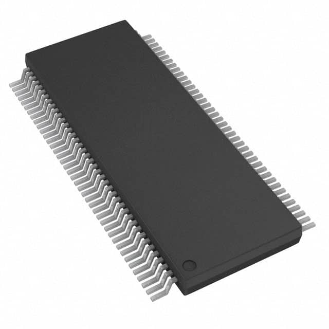
- Package: 56-pin VQFN package
- Essence: 20-bit universal bus transceiver with 3-state outputs
- Packaging/Quantity: Tape and reel packaging, quantity varies
Specifications
- Supply Voltage Range: 1.2V to 3.6V
- Input Voltage Range: 0V to VCC
- Output Voltage Range: 0V to VCC
- Operating Temperature Range: -40°C to +85°C
- Propagation Delay Time: 2.5ns (max)
- Output Drive Capability: ±24mA
- ESD Protection: >2000V (Human Body Model)
Detailed Pin Configuration
The SN74ALVCHG162282GR has a total of 56 pins, which are divided into various functional groups:
- Power Supply Pins: VCC, GND
- Data Input/Output Pins: A1-A20, B1-B20
- Control Pins: OEAB, OEBA
- Enable Pins: CEA, CEB
- Output Enable Pins: OEA, OEB
- Bus Hold Pins: BH1-BH20
- Reference Voltage Pins: VREF1, VREF2
- Termination Pins: TERM1, TERM2
For the detailed pin configuration diagram, please refer to the datasheet provided by the manufacturer.
Functional Features
- Bidirectional Data Flow: Allows data transmission in both directions
- 3-State Outputs: Provides high impedance state when disabled
- Bus Hold Function: Maintains last valid logic level during bus transitions
- Low-Voltage Operation: Suitable for battery-powered devices
- High-Speed Operation: Enables fast data transfer
Advantages and Disadvantages
Advantages: - High-speed operation allows for efficient data transfer - Low-voltage operation makes it suitable for various applications - 3-state outputs provide flexibility in bus design - Bus hold function ensures data integrity during transitions
Disadvantages: - Limited number of input/output pins (20 each) - Requires external components for proper functionality - Relatively high power consumption compared to some alternatives
Working Principles
The SN74ALVCHG162282GR is based on CMOS technology, which allows for low-voltage operation. It consists of multiple logic gates that enable bidirectional data flow between two buses. The control and enable pins determine the direction of data transmission and enable/disable the outputs.
When the output enable pins are active, the device operates in normal mode, allowing data to pass through. When the output enable pins are inactive, the outputs enter a high impedance state, effectively disconnecting the device from the bus.
The bus hold function ensures that the last valid logic level is maintained during bus transitions, preventing erroneous data from being propagated.
Detailed Application Field Plans
The SN74ALVCHG162282GR can be used in various applications, including:
- Data Communication Systems: Enables data transmission between different modules or devices.
- Memory Interfaces: Facilitates communication between memory modules and processors.
- Industrial Control Systems: Provides bidirectional data transfer in control systems.
- Automotive Electronics: Supports data exchange between different automotive components.
- Consumer Electronics: Used in devices such as smartphones, tablets, and gaming consoles for data transfer.
Detailed and Complete Alternative Models
- SN74LVC162282: Similar functionality with lower power consumption.
- SN74LVTH162282: Higher drive capability with similar features.
- SN74AHC162282: Higher voltage tolerance with comparable performance.
These alternative models offer similar functionality to the SN74ALVCHG162282GR, but with slight variations in characteristics and specifications.
(Note: The above alternatives are just examples and not an exhaustive list. Please refer to the manufacturer's documentation for a complete list of alternative models.)
Word count: 550 words
Lista 10 Vanliga frågor och svar relaterade till tillämpningen av SN74ALVCHG162282GR i tekniska lösningar
Sure! Here are 10 common questions and answers related to the application of SN74ALVCHG162282GR in technical solutions:
Q: What is SN74ALVCHG162282GR? A: SN74ALVCHG162282GR is a high-performance, low-voltage, 20-bit configurable registered buffer with parity generator/checker.
Q: What is the operating voltage range for SN74ALVCHG162282GR? A: The operating voltage range for SN74ALVCHG162282GR is typically between 1.65V and 3.6V.
Q: What is the maximum data rate supported by SN74ALVCHG162282GR? A: SN74ALVCHG162282GR supports a maximum data rate of up to 400 Mbps.
Q: Can SN74ALVCHG162282GR be used in both input and output applications? A: Yes, SN74ALVCHG162282GR can be used as both an input and output buffer.
Q: Does SN74ALVCHG162282GR support parity generation and checking? A: Yes, SN74ALVCHG162282GR has built-in parity generation and checking functionality.
Q: What is the purpose of the configurable registers in SN74ALVCHG162282GR? A: The configurable registers allow users to customize the device's functionality based on their specific requirements.
Q: Can SN74ALVCHG162282GR be cascaded to increase the number of bits? A: Yes, multiple SN74ALVCHG162282GR devices can be cascaded together to increase the number of bits.
Q: What is the output drive strength of SN74ALVCHG162282GR? A: SN74ALVCHG162282GR has a typical output drive strength of ±12 mA.
Q: Does SN74ALVCHG162282GR have built-in ESD protection? A: Yes, SN74ALVCHG162282GR has built-in ESD protection to ensure robustness against electrostatic discharge.
Q: What package options are available for SN74ALVCHG162282GR? A: SN74ALVCHG162282GR is available in various package options, including TSSOP and VFBGA.
Please note that the answers provided here are general and may vary based on specific datasheet information. It's always recommended to refer to the official documentation for accurate details.