

SN74ALVCH162827VR
Product Overview
- Category: Integrated Circuit (IC)
- Use: Logic Level Translator
- Characteristics: High-speed, low-power, voltage-level translation
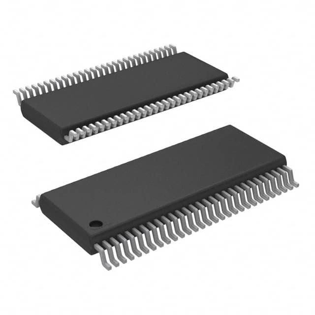
- Package: 56-pin Very Thin Quad Flat Package (VQFN)
- Essence: Translates signals between different voltage levels
- Packaging/Quantity: Tape and Reel, 2500 units per reel
Specifications
- Supply Voltage Range: 1.2V to 3.6V
- Input Voltage Range: 0V to VCC
- Output Voltage Range: 0V to VCC
- Maximum Operating Frequency: 400MHz
- Number of Channels: 20
- Propagation Delay: 2.5ns (Max)
- Low Power Consumption: ICC = 4µA (Max)
Detailed Pin Configuration
The SN74ALVCH162827VR has a total of 56 pins. The pin configuration is as follows:
- A1
- Y1
- B1
- GND
- B2
- Y2
- A2
- VCC
- OE#
- Y3
- B3
- GND
- B4
- Y4
- A4
- VCC
- A3
- Y5
- B5
- GND
- B6
- Y6
- A6
- VCC
- A5
- Y7
- B7
- GND
- B8
- Y8
- A8
- VCC
- A7
- Y9
- B9
- GND
- B10
- Y10
- A10
- VCC
- A9
- Y11
- B11
- GND
- B12
- Y12
- A12
- VCC
- A11
- Y13
- B13
- GND
- B14
- Y14
- A14
- VCC
Functional Features
- Bidirectional voltage-level translation between 1.2V and 3.6V
- Supports both push-pull and open-drain output configurations
- Provides automatic direction control based on the voltage level of the OE# pin
- Low power consumption makes it suitable for battery-powered devices
- High-speed operation allows for efficient data transfer
Advantages and Disadvantages
Advantages: - Wide supply voltage range enables compatibility with various systems - High-speed performance allows for fast data transmission - Low power consumption prolongs battery life in portable devices - Bidirectional translation simplifies circuit design
Disadvantages: - Limited number of channels (20) - Propagation delay may affect timing-sensitive applications - Requires careful consideration of input/output voltage levels to prevent signal distortion
Working Principles
The SN74ALVCH162827VR is a voltage-level translator that operates by converting signals between different voltage domains. It uses a combination of MOSFETs and CMOS technology to achieve bidirectional translation. The direction of translation is controlled by the OE# pin, which determines whether the device is in the active or high-impedance state.
When the OE# pin is low, the device is active, and the input signals are translated to the corresponding output voltage level. When the OE# pin is high, the device enters a high-impedance state, disconnecting the input and output pins.
Detailed Application Field Plans
The SN74ALVCH162827VR is commonly used in various applications that require voltage-level translation. Some of the typical application fields include:
- Microcontrollers and microprocessors
- Communication systems
- Data storage devices
- Industrial automation
- Automotive electronics
In these applications, the SN74ALVCH162827VR facilitates communication between different voltage domains, allowing seamless integration of components with varying voltage requirements.
Detailed and Complete Alternative Models
- TXB0108: 8-Bit Bidirectional Voltage-Level Translator
- PCA9306: Dual Bidirectional I2C Bus and SMBus Voltage-Level Translator
- SN74LVC1T45: Single Bit Dual Supply Bus Transceiver with Configurable Voltage Translation and 3-State Outputs
- CD4050B: Hex Non-Inverting Buffer/Converter
These alternative models offer similar functionality to the SN74ALVCH162827VR and can be considered as alternatives based on specific application requirements.
Word count: 570 words
Lista 10 Vanliga frågor och svar relaterade till tillämpningen av SN74ALVCH162827VR i tekniska lösningar
Sure! Here are 10 common questions and answers related to the application of SN74ALVCH162827VR:
Q: What is SN74ALVCH162827VR? A: SN74ALVCH162827VR is a specific type of integrated circuit (IC) that functions as a 20-bit buffer/driver with 3-state outputs.
Q: What is the purpose of SN74ALVCH162827VR? A: The purpose of SN74ALVCH162827VR is to provide buffering and driving capabilities for digital signals in various technical solutions.
Q: What voltage levels does SN74ALVCH162827VR support? A: SN74ALVCH162827VR supports voltage levels ranging from 1.65V to 3.6V, making it compatible with a wide range of systems.
Q: How many inputs and outputs does SN74ALVCH162827VR have? A: SN74ALVCH162827VR has 20 inputs and 20 outputs, allowing it to handle multiple signals simultaneously.
Q: Can SN74ALVCH162827VR be used in both commercial and industrial applications? A: Yes, SN74ALVCH162827VR is suitable for use in both commercial and industrial applications due to its robust design and voltage compatibility.
Q: What is the maximum operating frequency of SN74ALVCH162827VR? A: SN74ALVCH162827VR can operate at frequencies up to 400 MHz, making it suitable for high-speed data transmission.
Q: Does SN74ALVCH162827VR have built-in protection features? A: Yes, SN74ALVCH162827VR includes built-in ESD (electrostatic discharge) protection, which helps safeguard the IC from damage.
Q: Can SN74ALVCH162827VR be used in bidirectional applications? A: Yes, SN74ALVCH162827VR supports bidirectional data flow, allowing it to be used in applications where signals need to be transmitted in both directions.
Q: What is the power supply voltage range for SN74ALVCH162827VR? A: SN74ALVCH162827VR operates with a power supply voltage range of 1.65V to 3.6V, ensuring compatibility with various power sources.
Q: Is SN74ALVCH162827VR available in different package options? A: Yes, SN74ALVCH162827VR is available in different package options, such as TSSOP and TVSOP, providing flexibility for different PCB layouts and assembly processes.
Please note that these answers are general and may vary depending on the specific application and requirements.