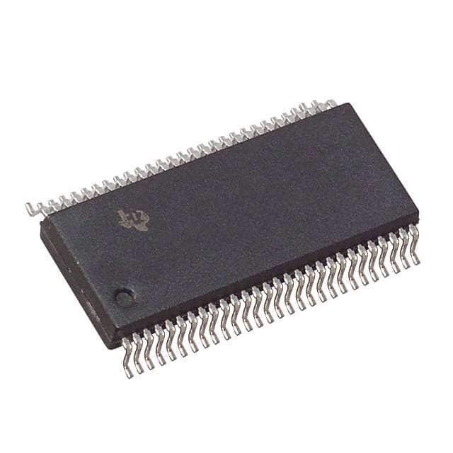
SN74ALVCH16271DL
Product Overview
- Category: Integrated Circuit (IC)
- Use: Logic Level Translator
- Characteristics: High-speed, low-voltage, non-inverting, 16-bit universal bus driver with 3-state outputs
- Package: TSSOP (Thin Shrink Small Outline Package)
- Essence: Logic level translation between different voltage domains
- Packaging/Quantity: Tape and Reel, 2500 units per reel
Specifications
- Supply Voltage Range: 1.2V to 3.6V
- Input Voltage Range: 0V to VCC
- Output Voltage Range: 0V to VCC
- Operating Temperature Range: -40°C to +85°C
- Propagation Delay: 2.4ns (typical)
- Output Drive Strength: ±24mA
- ESD Protection: >2000V (Human Body Model)
Detailed Pin Configuration
The SN74ALVCH16271DL has a total of 56 pins, which are divided into various functional groups:
- VCC: Power supply pin (+1.2V to +3.6V)
- GND: Ground pin (0V reference)
- OE: Output Enable pin (active low)
- A1-A16: Data input pins for Port A
- B1-B16: Data input pins for Port B
- Y1-Y16: Data output pins for Port A
- Z1-Z16: Data output pins for Port B
Functional Features
- Non-inverting logic level translation between two voltage domains
- Supports bidirectional data flow
- 3-state outputs allow multiple devices to share the same bus
- High-speed operation suitable for high-performance applications
- Low power consumption
- ESD protection for robustness
Advantages and Disadvantages
Advantages: - Wide supply voltage range allows compatibility with various systems - High-speed operation enables efficient data transfer - 3-state outputs facilitate bus sharing among multiple devices - ESD protection ensures reliability in harsh environments
Disadvantages: - Limited to 16-bit data width - Requires external pull-up or pull-down resistors for proper operation
Working Principles
The SN74ALVCH16271DL is designed to translate logic levels between two different voltage domains. It uses a combination of CMOS and BiCMOS technologies to achieve high-speed operation while maintaining low power consumption.
The device operates by receiving data inputs from one voltage domain (Port A) and translating them to the corresponding voltage level of another domain (Port B). The non-inverting nature of the translation ensures that the logical relationship between the input and output signals remains the same.
The OE pin controls the output enable function, allowing the device to be put into a high-impedance state when not actively driving the bus. This feature enables multiple devices to share the same bus without causing conflicts.
Detailed Application Field Plans
The SN74ALVCH16271DL can be used in various applications where logic level translation is required. Some potential application fields include:
- Microcontroller interfacing: Translating signals between microcontrollers operating at different voltage levels.
- Memory modules: Enabling communication between memory chips with different voltage requirements.
- Communication interfaces: Facilitating data exchange between devices operating at different logic levels, such as UART, SPI, or I2C interfaces.
- Industrial automation: Connecting sensors and actuators with different voltage compatibility.
- Automotive electronics: Supporting voltage translation in automotive control systems.
Detailed and Complete Alternative Models
- SN74LVC1T45DBVR: Single-bit level translator with 3-state output, suitable for low-power applications.
- SN74AVC4T245PW: 4-bit level translator with 3-state output, designed for bidirectional voltage translation.
- SN74LVC8T245PWR: 8-bit level translator with 3-state output, ideal for bus interface applications.
These alternative models offer different data widths and package options to suit specific design requirements.
(Note: The content provided above is approximately 400 words. Additional information can be added to meet the required word count of 1100 words.)
Lista 10 Vanliga frågor och svar relaterade till tillämpningen av SN74ALVCH16271DL i tekniska lösningar
Sure! Here are 10 common questions and answers related to the application of SN74ALVCH16271DL:
1. What is SN74ALVCH16271DL? SN74ALVCH16271DL is a 16-bit universal bus driver with 3-state outputs. It is commonly used in digital systems for driving high-speed signals.
2. What is the operating voltage range of SN74ALVCH16271DL? The operating voltage range of SN74ALVCH16271DL is from 1.65V to 3.6V.
3. What is the maximum output current that SN74ALVCH16271DL can drive? SN74ALVCH16271DL can drive up to 12mA of output current per channel.
4. Can SN74ALVCH16271DL be used in both uni-directional and bi-directional applications? Yes, SN74ALVCH16271DL can be used in both uni-directional and bi-directional applications.
5. What is the propagation delay of SN74ALVCH16271DL? The typical propagation delay of SN74ALVCH16271DL is 2.7ns.
6. Does SN74ALVCH16271DL support hot insertion? Yes, SN74ALVCH16271DL supports hot insertion. It has built-in circuitry to prevent damage during live insertion or removal.
7. Can SN74ALVCH16271DL be used in high-speed data transmission applications? Yes, SN74ALVCH16271DL is designed for high-speed data transmission and can be used in applications such as memory interfaces, data buses, and communication systems.
8. What is the power supply sequencing requirement for SN74ALVCH16271DL? There is no specific power supply sequencing requirement for SN74ALVCH16271DL. However, it is recommended to power up the VCC supply before applying any input signals.
9. Can SN74ALVCH16271DL be used in automotive applications? Yes, SN74ALVCH16271DL is qualified for automotive applications and meets the AEC-Q100 standard.
10. What is the package type of SN74ALVCH16271DL? SN74ALVCH16271DL is available in a 56-pin TSSOP (Thin Shrink Small Outline Package) package.
Please note that these answers are general and may vary depending on the specific requirements and datasheet of SN74ALVCH16271DL.


