

SN74ALVCH162344VR
Product Overview
- Category: Integrated Circuit (IC)
- Use: Logic Level Translator
- Characteristics: High-speed, low-voltage, 16-bit bus transceiver with 3-state outputs
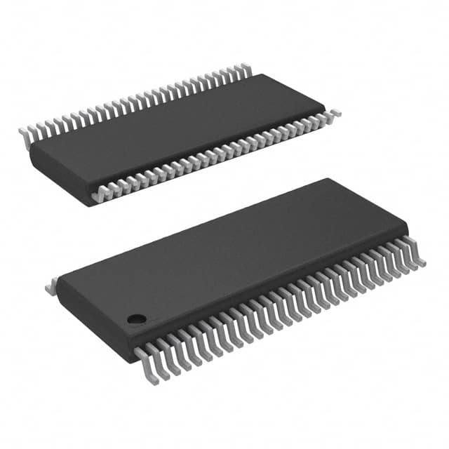
- Package: 56-pin Very Thin Quad Flat Package (VQFN)
- Essence: Translates signals between different voltage levels in digital systems
- Packaging/Quantity: Available in reels of 2500 units
Specifications
- Supply Voltage Range: 1.2V to 3.6V
- Input Voltage Range: 0V to VCC
- Output Voltage Range: 0V to VCC
- Maximum Operating Frequency: 400 MHz
- Number of Channels: 16
- Output Drive Strength: ±24 mA
- Propagation Delay: 2.5 ns (max)
Detailed Pin Configuration
The SN74ALVCH162344VR has a total of 56 pins. The pin configuration is as follows:
- OE (Output Enable) 1
- A1 (Input/Output) 1
- B1 (Input/Output) 1
- Y1 (Output) 1
- GND (Ground)
- Y2 (Output) 2
- B2 (Input/Output) 2
- A2 (Input/Output) 2
- OE (Output Enable) 2
- VCC (Supply Voltage)
- A3 (Input/Output) 3
- B3 (Input/Output) 3
- Y3 (Output) 3
- OE (Output Enable) 3
- A4 (Input/Output) 4
- B4 (Input/Output) 4
- Y4 (Output) 4
- GND (Ground)
- Y5 (Output) 5
- B5 (Input/Output) 5
- A5 (Input/Output) 5
- OE (Output Enable) 5
- VCC (Supply Voltage)
- OE (Output Enable) 6
- A6 (Input/Output) 6
- B6 (Input/Output) 6
- Y6 (Output) 6
- GND (Ground)
- Y7 (Output) 7
- B7 (Input/Output) 7
- A7 (Input/Output) 7
- OE (Output Enable) 7
- VCC (Supply Voltage)
- A8 (Input/Output) 8
- B8 (Input/Output) 8
- Y8 (Output) 8
- OE (Output Enable) 8
- A9 (Input/Output) 9
- B9 (Input/Output) 9
- Y9 (Output) 9
- GND (Ground)
- Y10 (Output) 10
- B10 (Input/Output) 10
- A10 (Input/Output) 10
- OE (Output Enable) 10
- VCC (Supply Voltage)
- OE (Output Enable) 11
- A11 (Input/Output) 11
- B11 (Input/Output) 11
- Y11 (Output) 11
- GND (Ground)
- Y12 (Output) 12
- B12 (Input/Output) 12
- A12 (Input/Output) 12
- OE (Output Enable) 12
- VCC (Supply Voltage)
Functional Features
- Bidirectional voltage translation between two different voltage domains
- Supports both level shifting and bus isolation
- 3-state outputs allow multiple devices to share a common bus
- High-speed operation with minimal propagation delay
- Low power consumption
Advantages and Disadvantages
Advantages: - Wide supply voltage range allows compatibility with various systems - High-speed operation enables efficient data transfer - 3-state outputs facilitate bus sharing among multiple devices - Low power consumption helps conserve energy
Disadvantages: - Limited number of channels (16) - Requires careful consideration of input and output voltage levels to avoid signal distortion
Working Principles
The SN74ALVCH162344VR is designed to translate digital signals between two voltage domains in a system. It utilizes a combination of level shifting and bus isolation techniques to ensure reliable communication between devices operating at different voltage levels.
The IC receives input signals from one domain and translates them to the corresponding voltage level of the other domain. The translated signals are then available at the output
Lista 10 Vanliga frågor och svar relaterade till tillämpningen av SN74ALVCH162344VR i tekniska lösningar
Sure! Here are 10 common questions and answers related to the application of SN74ALVCH162344VR:
Q: What is SN74ALVCH162344VR? A: SN74ALVCH162344VR is a 16-bit buffer/driver with 3-state outputs, designed for low-voltage (1.65V to 3.6V) applications.
Q: What is the maximum operating frequency of SN74ALVCH162344VR? A: The maximum operating frequency of SN74ALVCH162344VR is typically around 400 MHz.
Q: Can SN74ALVCH162344VR be used in both input and output applications? A: Yes, SN74ALVCH162344VR can be used as both an input buffer and an output driver.
Q: What is the purpose of the 3-state outputs in SN74ALVCH162344VR? A: The 3-state outputs allow multiple devices to share a common bus without interfering with each other.
Q: What is the voltage level compatibility of SN74ALVCH162344VR? A: SN74ALVCH162344VR is compatible with both TTL and CMOS voltage levels.
Q: Can SN74ALVCH162344VR handle bidirectional data flow? A: No, SN74ALVCH162344VR is a unidirectional buffer/driver and does not support bidirectional data flow.
Q: What is the typical output current capability of SN74ALVCH162344VR? A: SN74ALVCH162344VR has a typical output current capability of ±24 mA.
Q: Is SN74ALVCH162344VR suitable for high-speed data transmission? A: Yes, SN74ALVCH162344VR is designed for high-speed applications and can be used in data transmission systems.
Q: Can SN74ALVCH162344VR tolerate overvoltage conditions? A: No, SN74ALVCH162344VR is not designed to tolerate overvoltage conditions and may get damaged if exposed to voltages beyond its specified range.
Q: What is the package type of SN74ALVCH162344VR? A: SN74ALVCH162344VR is available in a 56-pin Very Thin Fine-Pitch Ball Grid Array (VFBGA) package.