

SN74ALVC245DGVR
Basic Information Overview
- Category: Integrated Circuit (IC)
- Use: Level Shifter and Bus Transceiver
- Characteristics: Bi-directional voltage level translation, high-speed operation, low power consumption
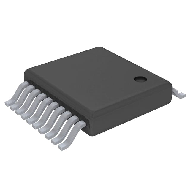
- Package: TSSOP-20
- Essence: Transfers data between different voltage domains in electronic systems
- Packaging/Quantity: Tape and Reel, 2500 units per reel
Specifications
- Supply Voltage Range: 1.65V to 3.6V
- Input Voltage Range: 0V to VCC
- Output Voltage Range: 0V to VCC
- Operating Temperature Range: -40°C to +85°C
- Maximum Data Rate: 400 Mbps
Detailed Pin Configuration
The SN74ALVC245DGVR has a total of 20 pins. The pin configuration is as follows:
Pin 1: A1
Pin 2: B1
Pin 3: GND
Pin 4: B2
Pin 5: A2
Pin 6: OE#
Pin 7: DIR
Pin 8: VCC
Pin 9: B3
Pin 10: A3
Pin 11: B4
Pin 12: A4
Pin 13: B5
Pin 14: A5
Pin 15: GND
Pin 16: B6
Pin 17: A6
Pin 18: B7
Pin 19: A7
Pin 20: VCC
Functional Features
- Bi-directional voltage level translation between two voltage domains
- High-speed operation allows for efficient data transfer
- Low power consumption for energy-efficient designs
- Enable input (OE#) controls the direction of data flow
- Supports bidirectional communication between different voltage systems
Advantages and Disadvantages
Advantages: - Efficient voltage level translation between different domains - High-speed operation for quick data transfer - Low power consumption for energy-efficient applications
Disadvantages: - Limited to a maximum data rate of 400 Mbps - Requires careful consideration of voltage compatibility between systems
Working Principles
The SN74ALVC245DGVR is designed to facilitate the transfer of data between electronic systems operating at different voltage levels. It acts as a bidirectional level shifter and bus transceiver, allowing seamless communication between two voltage domains.
The device operates by monitoring the input voltage levels and translating them to the appropriate output voltage levels. The direction of data flow is controlled by the enable input (OE#). When OE# is low, the device is enabled, and data can be transferred bidirectionally. When OE# is high, the device is disabled, and the data lines are in a high-impedance state.
Detailed Application Field Plans
The SN74ALVC245DGVR finds applications in various fields where voltage level translation and bus transceiver functionality are required. Some specific application areas include:
- Microcontroller Interfacing: The IC enables communication between microcontrollers operating at different voltage levels, facilitating seamless integration into larger systems.
- Communication Systems: It is used in communication systems to interface between different voltage domains, ensuring reliable data transfer.
- Industrial Automation: The device plays a crucial role in industrial automation systems, enabling communication between sensors, actuators, and control units operating at different voltage levels.
- Consumer Electronics: It is utilized in consumer electronics devices such as smartphones, tablets, and gaming consoles to enable communication between different subsystems.
Detailed and Complete Alternative Models
- TXB0108PWR: 8-Bit Bidirectional Voltage-Level Translator with Automatic Direction Sensing
- PCA9306DCTR: Dual Bidirectional I2C-Bus and SMBus Voltage-Level Translator
- SN74LVC8T245PWR: 8-Bit Dual-Supply Bus Transceiver with Configurable Voltage Translation
These alternative models offer similar functionality to the SN74ALVC245DGVR and can be considered as alternatives based on specific requirements.
In conclusion, the SN74ALVC245DGVR is an integrated circuit that serves as a level shifter and bus transceiver. It enables bidirectional voltage level translation between different voltage domains in electronic systems. With its high-speed operation, low power consumption, and compact TSSOP-20 package, it finds applications in various fields such as microcontroller interfacing, communication systems, industrial automation, and consumer electronics.
Lista 10 Vanliga frågor och svar relaterade till tillämpningen av SN74ALVC245DGVR i tekniska lösningar
Sure! Here are 10 common questions and answers related to the application of SN74ALVC245DGVR:
Q: What is SN74ALVC245DGVR? A: SN74ALVC245DGVR is a bidirectional octal bus transceiver with 3-state outputs, commonly used in digital systems.
Q: What is the voltage range supported by SN74ALVC245DGVR? A: SN74ALVC245DGVR supports a voltage range of 1.65V to 3.6V.
Q: How many data lines can SN74ALVC245DGVR handle? A: SN74ALVC245DGVR can handle 8 data lines, as it is an octal transceiver.
Q: Can SN74ALVC245DGVR be used for level shifting between different voltage domains? A: Yes, SN74ALVC245DGVR can be used for level shifting between different voltage domains due to its wide voltage range support.
Q: Does SN74ALVC245DGVR have any built-in protection features? A: Yes, SN74ALVC245DGVR has built-in ESD (Electrostatic Discharge) protection on all inputs and outputs.
Q: What is the maximum data transfer rate supported by SN74ALVC245DGVR? A: SN74ALVC245DGVR supports a maximum data transfer rate of 400 Mbps.
Q: Can SN74ALVC245DGVR be used in both parallel and serial communication systems? A: Yes, SN74ALVC245DGVR can be used in both parallel and serial communication systems, depending on the application requirements.
Q: Is SN74ALVC245DGVR compatible with other logic families? A: Yes, SN74ALVC245DGVR is compatible with a wide range of logic families, including TTL, CMOS, and LVCMOS.
Q: Can SN74ALVC245DGVR be used in both input and output modes simultaneously? A: No, SN74ALVC245DGVR operates in either input or output mode at a given time, depending on the control signals.
Q: What is the package type of SN74ALVC245DGVR? A: SN74ALVC245DGVR is available in a small form factor package called TSSOP-20.
Please note that these answers are general and may vary based on specific application requirements.