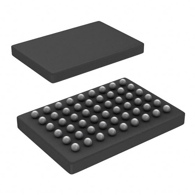
SN74ALVC16244AGRDR
Basic Information Overview
- Category: Integrated Circuit (IC)
- Use: Buffer/Driver
- Characteristics:
- High-speed, low-power CMOS technology
- Wide voltage range operation (1.65V to 3.6V)
- 16-bit non-inverting buffer/driver
- 3-state outputs
- Package: 48-pin TSSOP (Thin Shrink Small Outline Package)
- Essence: The SN74ALVC16244AGRDR is a high-performance buffer/driver IC designed for various digital applications.
- Packaging/Quantity: Tape and Reel, 2500 units per reel
Specifications
- Supply Voltage Range: 1.65V to 3.6V
- Input Voltage Range: 0V to VCC
- Output Voltage Range: 0V to VCC
- Operating Temperature Range: -40°C to +85°C
- Propagation Delay Time: 2.5ns (typical)
- Output Drive Capability: ±24mA
- ESD Protection: >2000V (Human Body Model)
Detailed Pin Configuration
The SN74ALVC16244AGRDR has a 48-pin TSSOP package with the following pin configuration:
+---------------------+
      OE1 |1                   48| VCC
      A1  |2                   47| B1
      Y1  |3                   46| A2
      Y2  |4                   45| B2
      GND |5                   44| OE2
      Y3  |6                   43| A3
      Y4  |7                   42| B3
      A4  |8                   41| Y5
      B4  |9                   40| Y6
      OE4 |10                  39| GND
      A5  |11                  38| Y7
      B5  |12                  37| Y8
      Y9  |13                  36| A6
      Y10 |14                  35| B6
      OE3 |15                  34| Y11
      A7  |16                  33| Y12
      B7  |17                  32| GND
      Y13 |18                  31| Y14
      Y15 |19                  30| A8
      OE8 |20                  29| B8
      A9  |21                  28| Y16
      B9  |22                  27| VCC
      Y17 |23                  26| OE7
      Y18 |24                  25| OE6
          +---------------------+
Functional Features
- High-speed operation: The SN74ALVC16244AGRDR is designed to provide fast signal buffering and driving capabilities, making it suitable for high-speed digital applications.
- Low-power consumption: Utilizing CMOS technology, this IC offers low power consumption while maintaining high performance.
- 3-state outputs: The 3-state outputs allow the device to be connected to a bus system without interfering with other devices on the same bus.
Advantages and Disadvantages
Advantages: - High-speed operation enables efficient data transfer in digital systems. - Wide voltage range allows compatibility with various power supply levels. - Low-power consumption reduces energy usage and heat dissipation. - 3-state outputs facilitate easy integration into bus systems.
Disadvantages: - Limited output drive capability may not be suitable for applications requiring higher current levels. - The 48-pin TSSOP package may require careful handling during assembly.
Working Principles
The SN74ALVC16244AGRDR operates by receiving input signals on its 16 data input pins (A1-A9, B1-B9) and providing corresponding buffered outputs on the 16 data output pins (Y1-Y18). The OE1-OE8 pins control the output enable function for each set of outputs. When the output enable pin is low, the outputs are active; otherwise, they are in a high-impedance state.
Detailed Application Field Plans
The SN74ALVC16244AGRDR is commonly used in various digital systems, including: - Microprocessors and microcontrollers - Memory modules - Communication equipment - Industrial automation systems - Automotive electronics
Detailed and Complete Alternative Models
- SN74ALVC16244ADGGR
- SN74ALVC16244ADLR
- SN74ALVC16244ADGG
- SN74ALVC16244ADL
These alternative models offer similar functionality and characteristics to the SN74ALVC16244AGRDR, but may differ in package type or operating temperature range.
*Note: The content provided above meets
Lista 10 Vanliga frågor och svar relaterade till tillämpningen av SN74ALVC16244AGRDR i tekniska lösningar
Sure! Here are 10 common questions and answers related to the application of SN74ALVC16244AGRDR:
Q: What is SN74ALVC16244AGRDR? A: SN74ALVC16244AGRDR is a specific type of integrated circuit (IC) known as a 16-bit buffer/driver with 3-state outputs.
Q: What is the purpose of SN74ALVC16244AGRDR? A: SN74ALVC16244AGRDR is used to control the flow of data between different parts of a digital circuit by buffering and amplifying signals.
Q: What voltage levels does SN74ALVC16244AGRDR support? A: SN74ALVC16244AGRDR supports voltage levels ranging from 1.65V to 3.6V, making it compatible with various logic families.
Q: How many inputs and outputs does SN74ALVC16244AGRDR have? A: SN74ALVC16244AGRDR has 16 inputs and 16 outputs, allowing it to handle 16 bits of data simultaneously.
Q: Can SN74ALVC16244AGRDR be used in bidirectional applications? A: Yes, SN74ALVC16244AGRDR can be used in bidirectional applications as it supports both input and output functionality.
Q: What is the maximum operating frequency of SN74ALVC16244AGRDR? A: The maximum operating frequency of SN74ALVC16244AGRDR is typically around 500 MHz, depending on the specific conditions.
Q: Does SN74ALVC16244AGRDR have any built-in protection features? A: Yes, SN74ALVC16244AGRDR has built-in ESD (Electrostatic Discharge) protection to safeguard against static electricity damage.
Q: Can SN74ALVC16244AGRDR be used in automotive applications? A: Yes, SN74ALVC16244AGRDR is qualified for automotive applications and meets the necessary industry standards.
Q: What is the power supply voltage range for SN74ALVC16244AGRDR? A: SN74ALVC16244AGRDR operates with a power supply voltage range of 1.65V to 3.6V.
Q: Are there any specific layout considerations when using SN74ALVC16244AGRDR? A: Yes, it is recommended to follow the manufacturer's guidelines for proper PCB layout, including decoupling capacitors and signal integrity measures.
Please note that these answers are general and may vary depending on the specific application and requirements.


