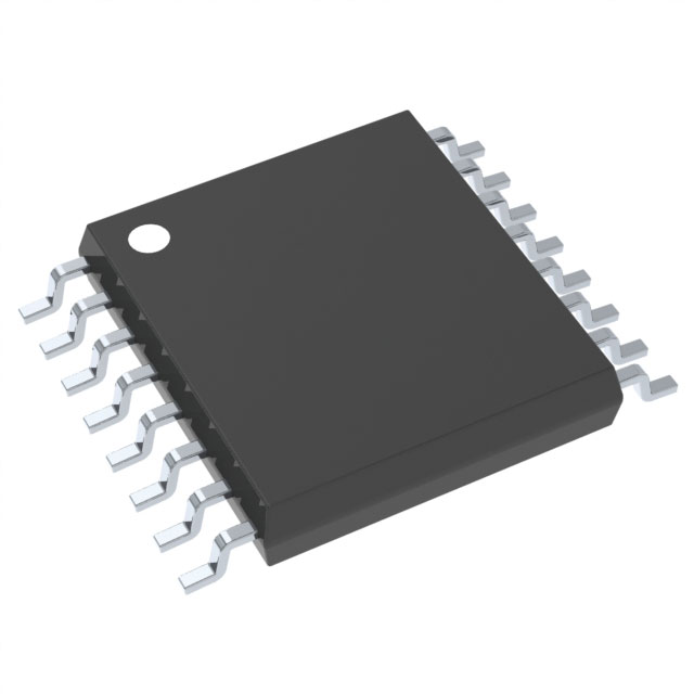
SN74AHCT595PWRG3
Product Overview
- Category: Integrated Circuit
- Use: Shift Register
- Characteristics: High-Speed, Low-Power, 8-Bit Serial-In, Parallel-Out
- Package: TSSOP (Thin Shrink Small Outline Package)
- Essence: Serial to Parallel Data Conversion
- Packaging/Quantity: Tape and Reel, 2500 pieces per reel
Specifications
- Supply Voltage Range: 2 V to 5.5 V
- Input Voltage Range: 0 V to VCC
- Output Voltage Range: 0 V to VCC
- Operating Temperature Range: -40°C to +85°C
- Maximum Clock Frequency: 100 MHz
- Number of Outputs: 8
- Number of Inputs: 1
- Number of Pins: 16
Detailed Pin Configuration
The SN74AHCT595PWRG3 has a total of 16 pins. The pin configuration is as follows:
- SER (Serial Data Input)
- OE (Output Enable)
- RCLK (Register Clock)
- SRCLK (Shift Register Clock)
- SRCLR (Shift Register Clear)
- QA (Output A)
- QB (Output B)
- QC (Output C)
- QD (Output D)
- QE (Output E)
- QF (Output F)
- QG (Output G)
- QH (Output H)
- GND (Ground)
- VCC (Supply Voltage)
- QH' (Serial Data Output)
Functional Features
- Serial-in, parallel-out shift register operation
- High-speed data transfer with a maximum clock frequency of 100 MHz
- Low-power consumption for energy-efficient applications
- Output enable control for easy interfacing with other devices
- Shift register clear function for resetting the register
- Wide supply voltage range for versatile usage
Advantages and Disadvantages
Advantages: - High-speed operation allows for quick data transfer - Low-power consumption makes it suitable for battery-powered devices - Compact TSSOP package saves board space - Output enable control enhances flexibility in system design
Disadvantages: - Limited number of outputs (8) - Requires external clock signals for proper operation
Working Principles
The SN74AHCT595PWRG3 is a shift register that converts serial data input into parallel output. It operates by shifting the input data bit-by-bit through the register upon receiving clock pulses. The shifted data is then available at the parallel output pins. The output enable pin allows the user to control when the output data is valid. The shift register clear pin resets the register, clearing all stored data.
Detailed Application Field Plans
The SN74AHCT595PWRG3 is widely used in various applications, including:
- LED Matrix Displays: The shift register can be used to control multiple LEDs in a matrix configuration, enabling dynamic lighting effects.
- Serial Data Expansion: It can be utilized to expand the number of digital inputs or outputs in microcontroller-based systems.
- Data Storage and Transfer: The shift register can be employed for temporary storage and transfer of data between different components in a system.
- Multiplexing: It enables multiplexing of multiple signals onto a single line, reducing the number of required connections.
Detailed and Complete Alternative Models
- 74HC595: Similar shift register with a wider supply voltage range (2 V to 6 V).
- CD4094: 8-stage shift-and-store bus register with complementary outputs.
- SN54HC595: High-speed CMOS shift register with similar functionality.
These alternative models offer similar features and can be considered as substitutes for the SN74AHCT595PWRG3 in various applications.
Word count: 529 words
Lista 10 Vanliga frågor och svar relaterade till tillämpningen av SN74AHCT595PWRG3 i tekniska lösningar
Sure! Here are 10 common questions and answers related to the application of SN74AHCT595PWRG3 in technical solutions:
Q: What is SN74AHCT595PWRG3? A: SN74AHCT595PWRG3 is a high-speed, 8-bit shift register with output latches. It can be used for serial-to-parallel data conversion or as a universal parallel-to-serial shift register.
Q: What is the operating voltage range of SN74AHCT595PWRG3? A: The operating voltage range of SN74AHCT595PWRG3 is from 4.5V to 5.5V.
Q: How many outputs does SN74AHCT595PWRG3 have? A: SN74AHCT595PWRG3 has 8 outputs that can drive up to 8 LEDs, relays, or other devices.
Q: Can SN74AHCT595PWRG3 be cascaded to control more than 8 outputs? A: Yes, SN74AHCT595PWRG3 can be cascaded to control multiple devices by connecting the serial output of one chip to the serial input of another.
Q: What is the maximum clock frequency supported by SN74AHCT595PWRG3? A: SN74AHCT595PWRG3 can operate at a maximum clock frequency of 100 MHz.
Q: Does SN74AHCT595PWRG3 have any built-in protection features? A: Yes, SN74AHCT595PWRG3 has built-in ESD protection on all inputs and outputs.
Q: Can SN74AHCT595PWRG3 be used with both CMOS and TTL logic levels? A: Yes, SN74AHCT595PWRG3 is compatible with both CMOS and TTL logic levels.
Q: What is the power consumption of SN74AHCT595PWRG3? A: The power consumption of SN74AHCT595PWRG3 depends on the operating frequency and load conditions but is typically low.
Q: Can SN74AHCT595PWRG3 be used in automotive applications? A: Yes, SN74AHCT595PWRG3 is qualified for automotive applications and meets the AEC-Q100 standard.
Q: Are there any application notes or reference designs available for SN74AHCT595PWRG3? A: Yes, Texas Instruments provides application notes and reference designs that can help in implementing SN74AHCT595PWRG3 in various technical solutions.
Please note that the answers provided here are general and may vary depending on specific requirements and use cases. It's always recommended to refer to the datasheet and documentation provided by the manufacturer for detailed information.


