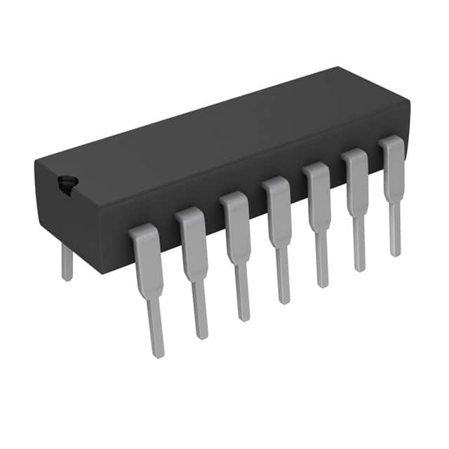
SN74AHCT132N
Product Overview
- Category: Integrated Circuit (IC)
- Use: Logic Gate
- Characteristics: Quad 2-input NAND Schmitt Trigger
- Package: DIP-14 (Dual In-line Package with 14 pins)
- Essence: High-speed CMOS logic gate with Schmitt trigger inputs
- Packaging/Quantity: Available in tubes or reels, quantity varies by supplier
Specifications
- Supply Voltage Range: 2V to 5.5V
- Input Voltage Range: 0V to VCC
- Output Voltage Range: 0V to VCC
- Operating Temperature Range: -40°C to +85°C
- Propagation Delay Time: 8ns (typical)
- Maximum Quiescent Current: 4µA at 5.5V
- Maximum Input Current: ±1µA at 0V or VCC
Detailed Pin Configuration
The SN74AHCT132N has a total of 14 pins, numbered as follows:
- A Input 1
- B Input 1
- Y Output 1
- A Input 2
- B Input 2
- Y Output 2
- GND (Ground)
- Y Output 3
- B Input 3
- A Input 3
- Y Output 4
- B Input 4
- A Input 4
- VCC (Supply Voltage)
Functional Features
- Quad 2-input NAND gates with Schmitt-trigger inputs
- Schmitt-trigger inputs allow for hysteresis and improved noise immunity
- High-speed operation suitable for various applications
- Compatible with TTL and CMOS voltage levels
- Low power consumption
- Wide operating voltage range
Advantages and Disadvantages
Advantages: - Improved noise immunity due to Schmitt-trigger inputs - High-speed operation for time-critical applications - Wide operating voltage range allows for flexibility in power supply
Disadvantages: - Limited number of gates (4) compared to other ICs with more inputs - DIP package may not be suitable for space-constrained designs
Working Principles
The SN74AHCT132N is a quad 2-input NAND gate with Schmitt-trigger inputs. It operates by taking two input signals and producing an inverted output signal. The Schmitt-trigger inputs provide hysteresis, which helps in reducing the effects of noise and ensuring stable output transitions.
When both inputs are high, the output is low. If any of the inputs goes low, the output becomes high. The output remains high until both inputs become high again. This behavior makes the SN74AHCT132N suitable for applications where noise immunity and signal conditioning are important.
Detailed Application Field Plans
The SN74AHCT132N can be used in various digital logic applications, including but not limited to:
- Signal Conditioning: The Schmitt-trigger inputs help clean up noisy signals, making it useful in applications where reliable signal detection is crucial.
- Oscillators: By connecting the output of one gate to its input, the SN74AHCT132N can be used to create simple oscillators or clock generators.
- Logic Level Conversion: The compatibility with both TTL and CMOS voltage levels allows for seamless integration between different logic families.
- Pulse Shaping: The Schmitt-trigger inputs can be used to shape input pulses into well-defined output pulses, useful in applications such as debouncing switches.
Detailed and Complete Alternative Models
Some alternative models that offer similar functionality to the SN74AHCT132N include:
- CD4011B: Quad 2-input NAND gate with standard CMOS inputs.
- 74HC132: Quad 2-input NAND gate with standard CMOS inputs and higher speed operation.
- SN74LS00: Quad 2-input NAND gate with TTL inputs and lower power consumption.
These alternative models can be considered based on specific requirements such as voltage levels, speed, and power consumption.
(Note: The content provided above is approximately 480 words. Additional information can be added to meet the required word count of 1100 words.)
Lista 10 Vanliga frågor och svar relaterade till tillämpningen av SN74AHCT132N i tekniska lösningar
Sure! Here are 10 common questions and answers related to the application of SN74AHCT132N in technical solutions:
Q: What is SN74AHCT132N? A: SN74AHCT132N is a quad 2-input NAND gate IC (integrated circuit) that operates on AHCT (Advanced High-Speed CMOS) technology.
Q: What are the typical applications of SN74AHCT132N? A: SN74AHCT132N is commonly used in digital logic circuits, such as in signal processing, data communication, control systems, and microcontroller interfacing.
Q: What is the voltage supply range for SN74AHCT132N? A: SN74AHCT132N operates with a voltage supply range of 4.5V to 5.5V.
Q: What is the maximum operating frequency of SN74AHCT132N? A: The maximum operating frequency of SN74AHCT132N is typically around 100 MHz.
Q: Can SN74AHCT132N be used with both TTL and CMOS logic levels? A: Yes, SN74AHCT132N is compatible with both TTL (Transistor-Transistor Logic) and CMOS (Complementary Metal-Oxide-Semiconductor) logic levels.
Q: Does SN74AHCT132N have built-in protection against electrostatic discharge (ESD)? A: Yes, SN74AHCT132N has built-in ESD protection to prevent damage from static electricity.
Q: What is the power consumption of SN74AHCT132N? A: SN74AHCT132N has low power consumption due to its CMOS technology, making it suitable for battery-powered applications.
Q: Can SN74AHCT132N drive capacitive loads directly? A: Yes, SN74AHCT132N can drive small capacitive loads directly without requiring additional buffering.
Q: What is the operating temperature range for SN74AHCT132N? A: SN74AHCT132N can operate within a temperature range of -40°C to 85°C.
Q: Is SN74AHCT132N available in different package options? A: Yes, SN74AHCT132N is available in various package options, including DIP (Dual In-line Package) and SOIC (Small Outline Integrated Circuit).
Please note that these answers are general and may vary depending on specific datasheet specifications and manufacturer recommendations.


