

SN74AHC74RGYR
Product Overview
- Category: Integrated Circuit (IC)
- Use: Flip-Flop
- Characteristics: High-Speed, Low-Power, Dual D-Type Positive-Edge-Triggered Flip-Flop
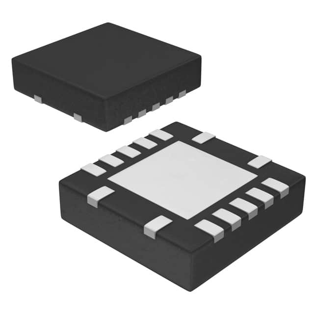
- Package: 14-VQFN (3.5mm x 3.5mm)
- Essence: This IC is a dual D-type flip-flop that operates at high speed while consuming low power. It is designed to be triggered on the positive edge of the clock signal.
- Packaging/Quantity: Available in reels with 2500 units per reel.
Specifications
- Supply Voltage Range: 2V to 5.5V
- High-Speed Operation: 8ns maximum propagation delay
- Low Power Consumption: ICC = 4µA maximum
- Operating Temperature Range: -40°C to +85°C
- Output Drive Capability: ±24mA at 3.3V
- Input Voltage Levels: VIL = 0.8V, VIH = 2V
- Pin Count: 14
Detailed Pin Configuration
The SN74AHC74RGYR has a total of 14 pins, which are assigned specific functions as follows:
- CLR (Clear) - Active LOW clear input
- D1 (Data Input 1) - Data input for flip-flop 1
- CLK (Clock) - Clock input
- D2 (Data Input 2) - Data input for flip-flop 2
- Q1 (Output 1) - Output of flip-flop 1
- Q1̅ (Complementary Output 1) - Complementary output of flip-flop 1
- GND (Ground) - Ground reference
- Q2 (Output 2) - Output of flip-flop 2
- Q2̅ (Complementary Output 2) - Complementary output of flip-flop 2
- PRE (Preset) - Active LOW preset input
- PR̅E (Complementary Preset) - Active HIGH complementary preset input
- CLR̅ (Complementary Clear) - Active HIGH complementary clear input
- VCC (Supply Voltage) - Positive supply voltage
- OE (Output Enable) - Active LOW output enable input
Functional Features
- Dual D-Type Flip-Flop: The SN74AHC74RGYR consists of two independent D-type flip-flops, allowing for the storage and transfer of data.
- Positive-Edge Triggered: The flip-flops are triggered on the positive edge of the clock signal, ensuring accurate timing and synchronization.
- Clear and Preset Inputs: The IC provides clear and preset inputs to initialize the flip-flop outputs to a known state.
- Output Enable Control: The output enable input allows for the activation or deactivation of the flip-flop outputs.
Advantages and Disadvantages
Advantages: - High-Speed Operation: The IC offers fast propagation delay, making it suitable for applications requiring quick data storage and transfer. - Low Power Consumption: With a maximum current consumption of 4µA, the IC is energy-efficient and helps prolong battery life in portable devices. - Small Package Size: The 14-VQFN package with dimensions of 3.5mm x 3.5mm enables space-saving integration in compact electronic designs.
Disadvantages: - Limited Functionality: The IC is specifically designed as a dual D-type flip-flop and may not be suitable for applications requiring more complex logic functions. - Single Supply Voltage Range: The operating voltage range of 2V to 5.5V may limit compatibility with certain systems that require higher or lower voltages.
Working Principles
The SN74AHC74RGYR operates based on the principles of D-type flip-flops. When the clock input (CLK) receives a positive edge, the data inputs (D1 and D2) are transferred to the corresponding outputs (Q1 and Q2). The clear (CLR) and preset (PRE) inputs allow for initialization of the flip-flop outputs to a known state. The output enable (OE) input controls the activation or deactivation of the flip-flop outputs.
Detailed Application Field Plans
The SN74AHC74RGYR can be utilized in various applications, including but not limited to:
- Digital Communication Systems: Used for data storage and synchronization in communication protocols such as UART, SPI, and I2C.
- Microcontroller and FPGA Designs: Employed for register-based operations, state machine implementations, and synchronization between different modules.
- Signal Processing Circuits: Utilized in digital filters, signal generators, and waveform shaping circuits.
- Timing and Control Circuits: Integrated into systems requiring precise timing control, such as clock dividers
Lista 10 Vanliga frågor och svar relaterade till tillämpningen av SN74AHC74RGYR i tekniska lösningar
Sure! Here are 10 common questions and answers related to the application of SN74AHC74RGYR in technical solutions:
Q: What is the SN74AHC74RGYR? A: The SN74AHC74RGYR is a dual positive-edge-triggered D-type flip-flop IC (integrated circuit) with reset, manufactured by Texas Instruments.
Q: What is the purpose of the SN74AHC74RGYR? A: The SN74AHC74RGYR is commonly used for storing and transferring binary data in digital circuits. It can be used in various applications such as counters, registers, and memory units.
Q: What is the operating voltage range of the SN74AHC74RGYR? A: The SN74AHC74RGYR operates within a voltage range of 2 V to 5.5 V.
Q: How many flip-flops are there in the SN74AHC74RGYR? A: The SN74AHC74RGYR contains two independent D-type flip-flops.
Q: What is the maximum clock frequency supported by the SN74AHC74RGYR? A: The SN74AHC74RGYR can operate at a maximum clock frequency of 100 MHz.
Q: Does the SN74AHC74RGYR have a reset function? A: Yes, the SN74AHC74RGYR has an asynchronous active-low reset input (CLR) that allows resetting the flip-flops to a known state.
Q: What is the output drive capability of the SN74AHC74RGYR? A: The SN74AHC74RGYR has a typical output drive capability of ±8 mA.
Q: Can the SN74AHC74RGYR be used in both CMOS and TTL logic systems? A: Yes, the SN74AHC74RGYR is compatible with both CMOS and TTL logic levels, making it versatile for various applications.
Q: What is the package type of the SN74AHC74RGYR? A: The SN74AHC74RGYR is available in a small-outline integrated circuit (SOIC) package.
Q: Are there any specific precautions to consider when using the SN74AHC74RGYR? A: It is important to follow the recommended operating conditions and guidelines provided in the datasheet to ensure proper functionality and reliability of the SN74AHC74RGYR.