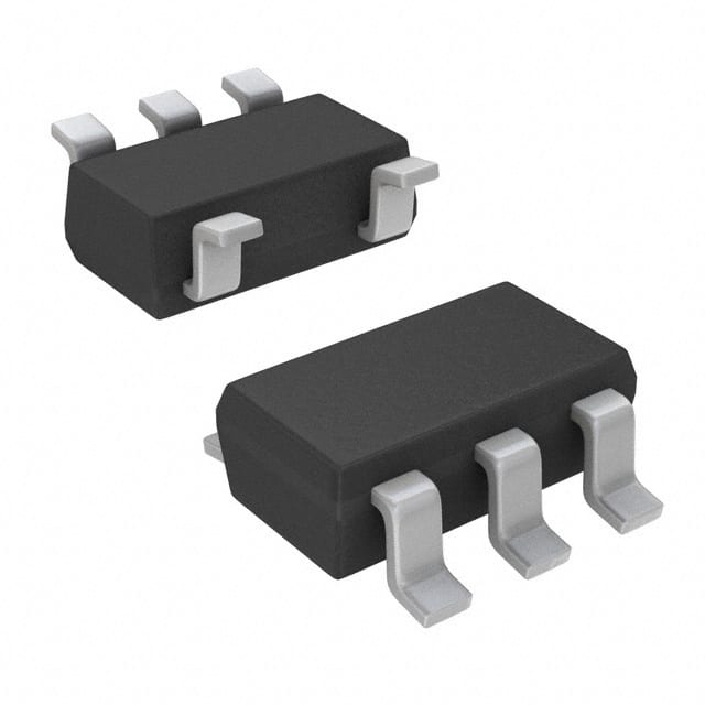
SN74AHC1G126DCKT
Product Overview
- Category: Integrated Circuit
- Use: Logic Gate Buffer/Driver
- Characteristics: Single Gate, Non-Inverting, 3-State Output
- Package: SC-70 (6-Lead), VSSOP (6-Lead)
- Essence: High-Speed CMOS Technology
- Packaging/Quantity: Tape and Reel, 2500 Units per Reel
Specifications
- Supply Voltage Range: 2 V to 5.5 V
- Input Voltage Range: 0 V to VCC
- Output Voltage Range: 0 V to VCC
- Operating Temperature Range: -40°C to +85°C
- Propagation Delay: 4.5 ns (Max) at 5 V
- Output Drive Capability: ±8 mA at 5 V
- Input Capacitance: 3 pF (Typical)
Pin Configuration
The SN74AHC1G126DCKT has a total of 6 pins arranged as follows:
____
   1 |o    |
   2 |     |
   3 |     |
   4 |     |
   5 |     |
   6 |____o|
Pin Description:
- GND: Ground
- A: Input
- OE: Output Enable
- Y: Output
- NC: No Connection
- VCC: Power Supply
Functional Features
- Single non-inverting buffer/driver with 3-state output
- High-speed operation suitable for various applications
- Wide supply voltage range allows compatibility with different systems
- Low power consumption
- Schmitt-trigger input for noise immunity
- ESD protection on all inputs and outputs
Advantages
- Small package size allows for space-saving designs
- High-speed operation enables efficient data transmission
- 3-state output provides flexibility in controlling bus lines
- Wide supply voltage range enhances compatibility with different systems
- ESD protection ensures reliability in harsh environments
Disadvantages
- Limited number of gates per package (single gate)
- Not suitable for applications requiring multiple gates or complex logic functions
Working Principles
The SN74AHC1G126DCKT is a single non-inverting buffer/driver integrated circuit. It takes an input signal and amplifies it to drive an output signal. The 3-state output feature allows the output to be disconnected from the bus line, providing flexibility in controlling the flow of data.
The device operates using high-speed CMOS technology, which ensures fast switching times and low power consumption. It has a wide supply voltage range, making it compatible with various systems. The Schmitt-trigger input provides noise immunity, allowing reliable operation even in noisy environments.
Detailed Application Field Plans
The SN74AHC1G126DCKT is commonly used in various applications, including:
- Communication Systems: It can be used as a buffer/driver in communication systems to amplify and transmit signals between different components.
- Industrial Automation: The device finds application in industrial automation systems where it helps control and drive various actuators and sensors.
- Consumer Electronics: It is used in consumer electronic devices such as smartphones, tablets, and gaming consoles to interface with external peripherals.
- Automotive Electronics: The IC is suitable for automotive electronics applications, including vehicle control systems, infotainment systems, and sensor interfaces.
Alternative Models
- SN74AHC1G125DBVR: Single non-inverting buffer/driver with 3-state output, SOT-23 package.
- SN74AHC1G07DCKR: Single non-inverting buffer/driver with open-drain output, SC-70 package.
- SN74AHC1G08DCKR: Single 2-input AND gate, SC-70 package.
These alternative models offer similar functionality and can be used as substitutes for the SN74AHC1G126DCKT in different applications.
Note: The above information is subject to change. Please refer to the manufacturer's datasheet for the most up-to-date specifications and details.
Lista 10 Vanliga frågor och svar relaterade till tillämpningen av SN74AHC1G126DCKT i tekniska lösningar
Sure! Here are 10 common questions and answers related to the application of SN74AHC1G126DCKT:
Q1: What is SN74AHC1G126DCKT? A1: SN74AHC1G126DCKT is a single bus buffer gate with 3-state output. It is commonly used in digital logic circuits for signal buffering and level shifting.
Q2: What is the operating voltage range of SN74AHC1G126DCKT? A2: The operating voltage range of SN74AHC1G126DCKT is from 2 V to 5.5 V.
Q3: What is the maximum output current of SN74AHC1G126DCKT? A3: The maximum output current of SN74AHC1G126DCKT is 8 mA.
Q4: Can SN74AHC1G126DCKT be used as a level shifter? A4: Yes, SN74AHC1G126DCKT can be used as a level shifter to convert signals between different voltage levels.
Q5: How many inputs does SN74AHC1G126DCKT have? A5: SN74AHC1G126DCKT has one input.
Q6: What is the propagation delay of SN74AHC1G126DCKT? A6: The propagation delay of SN74AHC1G126DCKT is typically around 4 ns.
Q7: Can SN74AHC1G126DCKT drive capacitive loads? A7: Yes, SN74AHC1G126DCKT can drive capacitive loads up to 50 pF.
Q8: Is SN74AHC1G126DCKT compatible with other logic families? A8: Yes, SN74AHC1G126DCKT is compatible with both CMOS and TTL logic families.
Q9: Can SN74AHC1G126DCKT be used in high-speed applications? A9: Yes, SN74AHC1G126DCKT can be used in high-speed applications as it has a maximum propagation delay of 4 ns.
Q10: What is the package type of SN74AHC1G126DCKT? A10: SN74AHC1G126DCKT comes in a SC-70 (DCK) package.
Please note that these answers are general and may vary depending on specific datasheet specifications.


