

LMK04906BISQ/NOPB
Product Overview
Category: Integrated Circuit (IC)
Use: The LMK04906BISQ/NOPB is a high-performance clock jitter cleaner and frequency synthesizer IC. It is designed to provide precise clock signals with low jitter for various applications in electronic devices.
Characteristics: - High-performance clock jitter cleaning - Frequency synthesis capability - Low jitter output signals - Wide operating frequency range - Compact package size - Easy integration into electronic circuits
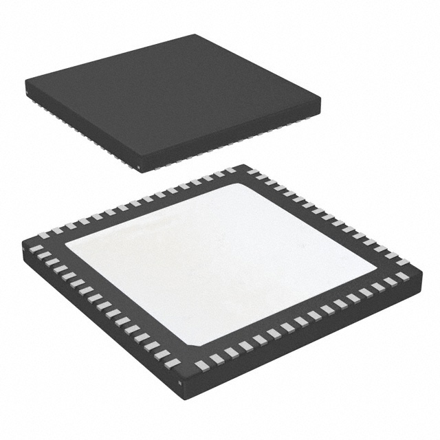
Package: The LMK04906BISQ/NOPB is available in a small outline integrated circuit (SOIC) package, which ensures easy installation and integration into electronic systems.
Essence: The essence of the LMK04906BISQ/NOPB lies in its ability to generate highly accurate clock signals with minimal jitter, making it suitable for demanding applications that require precise timing.
Packaging/Quantity: The LMK04906BISQ/NOPB is typically sold in reels or tubes containing a specific quantity of ICs, depending on the manufacturer's packaging standards.
Specifications
- Operating Voltage: 3.3V
- Operating Temperature Range: -40°C to +85°C
- Output Clock Frequency Range: 1MHz to 2.67GHz
- Jitter Performance: <1 ps RMS (Root Mean Square)
- Input Reference Clock Frequency Range: 10kHz to 710MHz
- Power Consumption: <300mW
Detailed Pin Configuration
The LMK04906BISQ/NOPB features a total of 32 pins, each serving a specific function. The pin configuration is as follows:
- VDDA: Analog power supply voltage
- VSSA: Analog ground
- VDDC: Core power supply voltage
- VSSC: Core ground
- VDDP: PLL power supply voltage
- VSSP: PLL ground
- XTALN: Crystal oscillator input (negative)
- XTALP: Crystal oscillator input (positive)
- REFCLK1P: Reference clock 1 positive input
- REFCLK1N: Reference clock 1 negative input
- REFCLK2P: Reference clock 2 positive input
- REFCLK2N: Reference clock 2 negative input
- CLKINP: Clock input positive
- CLKINN: Clock input negative
- CLKOUT0: Clock output 0
- CLKOUT1: Clock output 1
- CLKOUT2: Clock output 2
- CLKOUT3: Clock output 3
- CLKOUT4: Clock output 4
- CLKOUT5: Clock output 5
- CLKOUT6: Clock output 6
- CLKOUT7: Clock output 7
- CLKOUT8: Clock output 8
- CLKOUT9: Clock output 9
- CLKOUT10: Clock output 10
- CLKOUT11: Clock output 11
- CLKOUT12: Clock output 12
- CLKOUT13: Clock output 13
- CLKOUT14: Clock output 14
- CLKOUT15: Clock output 15
- NC: No connection
- NC: No connection
Functional Features
The LMK04906BISQ/NOPB offers the following functional features:
- Jitter Cleaning: The IC employs advanced techniques to reduce clock jitter, resulting in cleaner and more accurate clock signals.
- Frequency Synthesis: It can generate a wide range of frequencies, making it versatile for various applications.
- Multiple Clock Outputs: The IC provides multiple clock outputs, allowing for flexible signal distribution in complex systems.
- Low Power Consumption: The LMK04906BISQ/NOPB is designed to operate efficiently with low power consumption, making it suitable for battery-powered devices.
Advantages and Disadvantages
Advantages: - High-performance clock jitter cleaning ensures precise timing in electronic systems. - Wide operating frequency range allows for versatile applications. - Compact package size facilitates easy integration into electronic circuits. - Multiple clock outputs provide flexibility in signal distribution.
Disadvantages: - Limited pin count may restrict the number of simultaneous clock outputs in complex systems. - Requires external crystal oscillator or reference clock source for operation.
Working Principles
The LMK04906BISQ/NOPB utilizes a combination of phase-locked loop (PLL) and clock jitter cleaning techniques to generate accurate clock signals. It takes an input reference clock and processes it through the PLL to generate a stable output clock with reduced jitter. The IC also offers frequency synthesis capabilities, allowing for the generation of various frequencies based on the input reference.
Detailed Application Field Plans
The LMK049
Lista 10 Vanliga frågor och svar relaterade till tillämpningen av LMK04906BISQ/NOPB i tekniska lösningar
What is the typical input voltage range for LMK04906BISQ/NOPB?
- The typical input voltage range for LMK04906BISQ/NOPB is 2.5V to 3.3V.What is the maximum output frequency of LMK04906BISQ/NOPB?
- The maximum output frequency of LMK04906BISQ/NOPB is 1.5 GHz.Can LMK04906BISQ/NOPB be used in clock distribution applications?
- Yes, LMK04906BISQ/NOPB is suitable for clock distribution applications.What are the key features of LMK04906BISQ/NOPB?
- The key features of LMK04906BISQ/NOPB include low additive jitter, integrated phase-locked loop (PLL), and multiple outputs.Is LMK04906BISQ/NOPB suitable for use in telecommunications equipment?
- Yes, LMK04906BISQ/NOPB is suitable for use in telecommunications equipment.What is the operating temperature range for LMK04906BISQ/NOPB?
- The operating temperature range for LMK04906BISQ/NOPB is -40°C to 85°C.Can LMK04906BISQ/NOPB be powered by a single supply voltage?
- Yes, LMK04906BISQ/NOPB can be powered by a single supply voltage.Does LMK04906BISQ/NOPB support frequency synchronization?
- Yes, LMK04906BISQ/NOPB supports frequency synchronization.What is the package type of LMK04906BISQ/NOPB?
- LMK04906BISQ/NOPB is available in a 32-pin WQFN package.Are evaluation modules available for LMK04906BISQ/NOPB?
- Yes, evaluation modules are available for LMK04906BISQ/NOPB.