

DS50PCI401SQE/NOPB
Product Overview
- Category: Integrated Circuit
- Use: Signal Conditioning and Data Transmission
- Characteristics: High-speed, Low-power, Differential Signaling
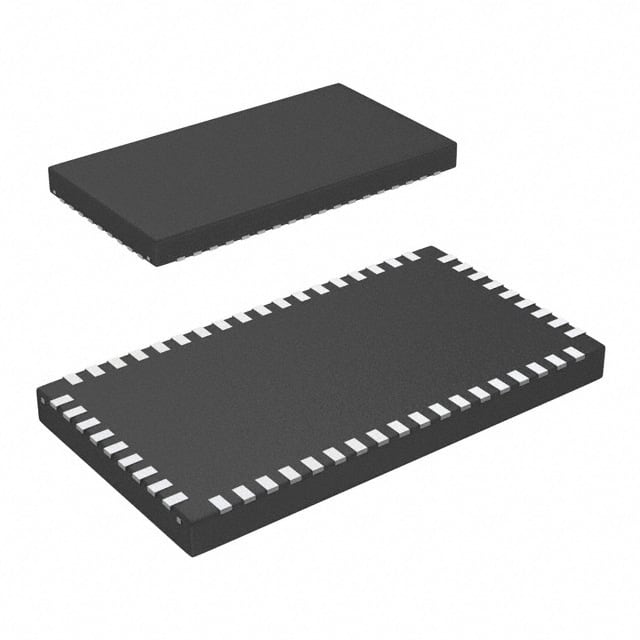
- Package: 48-pin LLP (Leadless Leadframe Package)
- Essence: Signal conditioning and data transmission for high-speed digital communication systems
- Packaging/Quantity: Tape and Reel, 2500 units per reel
Specifications
- Supply Voltage: 3.3V ±10%
- Operating Temperature Range: -40°C to +85°C
- Data Rate: Up to 5 Gbps
- Number of Channels: 4
- Input Interface: LVDS (Low-Voltage Differential Signaling)
- Output Interface: CML (Current Mode Logic)
- Package Dimensions: 7mm x 7mm
Pin Configuration
The DS50PCI401SQE/NOPB has a total of 48 pins. The pin configuration is as follows:
- VCC
- VCC
- GND
- GND
- Channel 1 LVDS Input
- Channel 1 LVDS Input
- Channel 1 LVDS Output
- Channel 1 LVDS Output
- Channel 2 LVDS Input
- Channel 2 LVDS Input
- Channel 2 LVDS Output
- Channel 2 LVDS Output
- Channel 3 LVDS Input
- Channel 3 LVDS Input
- Channel 3 LVDS Output
- Channel 3 LVDS Output
- Channel 4 LVDS Input
- Channel 4 LVDS Input
- Channel 4 LVDS Output
- Channel 4 LVDS Output
- GND
- GND
- VCC
- VCC
- CML Output Enable
- CML Output Enable
- CML Output Enable
- CML Output Enable
- CML Output 1
- CML Output 1
- CML Output 2
- CML Output 2
- CML Output 3
- CML Output 3
- CML Output 4
- CML Output 4
- GND
- GND
- VCC
- VCC
- CML Input 1
- CML Input 1
- CML Input 2
- CML Input 2
- CML Input 3
- CML Input 3
- CML Input 4
- CML Input 4
Functional Features
- Signal conditioning for high-speed digital communication systems
- Differential signaling for noise immunity
- Low-power consumption
- High data rate transmission up to 5 Gbps
- Integrated termination resistors for LVDS inputs
- CML outputs for compatibility with downstream devices
Advantages and Disadvantages
Advantages
- High-speed data transmission capability
- Low power consumption
- Integrated termination resistors simplify system design
- Differential signaling provides noise immunity
Disadvantages
- Limited number of channels (4)
- Requires LVDS input and CML output interfaces
Working Principles
The DS50PCI401SQE/NOPB is designed to condition and transmit high-speed digital signals in a differential manner. It accepts LVDS input signals from the source and conditions them for transmission through CML outputs. The integrated termination resistors ensure signal integrity and simplify system design.
Application Field Plans
The DS50PCI401SQE/NOPB is commonly used in applications that require high-speed data transmission with low power consumption. Some potential application fields include:
- High-speed communication systems
- Data centers and server farms
- Telecommunications equipment
- Industrial automation and control systems
- Medical imaging devices
Alternative Models
- DS50PCI401SQE/NOPB: 4-channel differential signal conditioner and transmitter (current model)
- DS50PCI400SQE/NOPB: 4-channel differential signal conditioner and transmitter (previous model)
- DS50PCI402SQE/NOPB: 8-channel differential signal conditioner and transmitter
- DS50PCI403SQE/NOPB: 16-channel differential signal conditioner and transmitter
These alternative models offer varying channel counts to suit different application requirements.
Word count: 498 words
Lista 10 Vanliga frågor och svar relaterade till tillämpningen av DS50PCI401SQE/NOPB i tekniska lösningar
What is the maximum data rate supported by DS50PCI401SQE/NOPB?
- The maximum data rate supported by DS50PCI401SQE/NOPB is 6.25 Gbps per lane.Can DS50PCI401SQE/NOPB be used in automotive applications?
- Yes, DS50PCI401SQE/NOPB is AEC-Q100 qualified and suitable for automotive applications.What is the power supply voltage range for DS50PCI401SQE/NOPB?
- The power supply voltage range for DS50PCI401SQE/NOPB is 1.8V to 3.3V.Does DS50PCI401SQE/NOPB support spread spectrum clocking?
- Yes, DS50PCI401SQE/NOPB supports spread spectrum clocking for reduced EMI.Can DS50PCI401SQE/NOPB be used in industrial control systems?
- Yes, DS50PCI401SQE/NOPB is suitable for use in industrial control systems.What is the operating temperature range for DS50PCI401SQE/NOPB?
- The operating temperature range for DS50PCI401SQE/NOPB is -40°C to 85°C.Is DS50PCI401SQE/NOPB compatible with PCIe Gen2 and Gen3 standards?
- Yes, DS50PCI401SQE/NOPB is compatible with PCIe Gen2 and Gen3 standards.Does DS50PCI401SQE/NOPB support hot-plug capability?
- Yes, DS50PCI401SQE/NOPB supports hot-plug capability for ease of use.Can DS50PCI401SQE/NOPB be used in medical imaging equipment?
- Yes, DS50PCI401SQE/NOPB is suitable for use in medical imaging equipment.What is the package type for DS50PCI401SQE/NOPB?
- DS50PCI401SQE/NOPB is available in a 48-pin WQFN package.